Horizontal InAs nanowire transistors grown on patterned silicon-on-insulator substrate
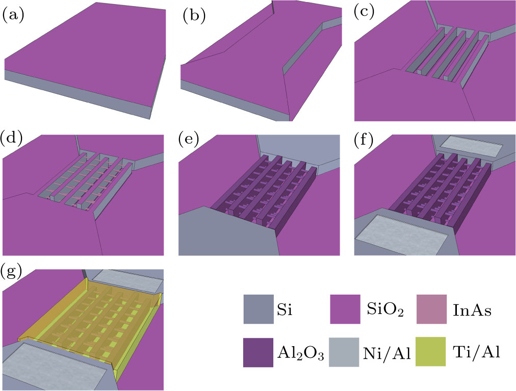
(color online) Schematics illustrating the fabrication process flow. (a) Dry oxidation and ion implantation. (b) Formation of dumbbell-like isolation. (c) Defining the interdigital structure on the top Si layer. (d) Epitaxy of horizontal InAs nanowires by MOCVD. (e) Deposition of Al2O3 gate dielectrcs on InAs nanowires. (f) Metal doposition and ohmic contact for S/D. (g) Gate electrode doposition.