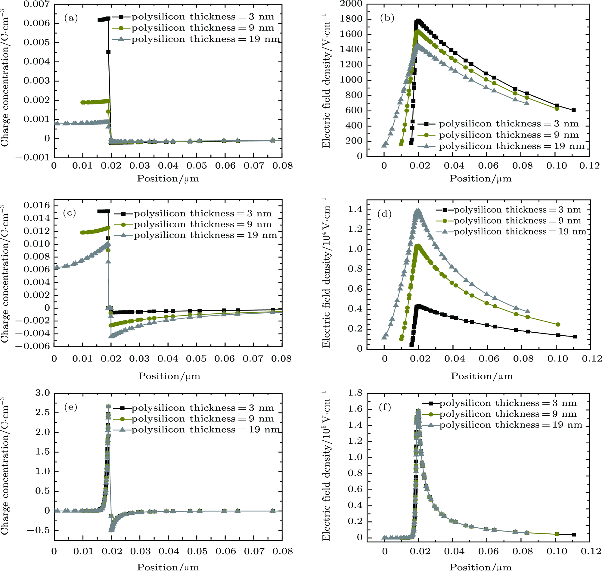
Studies on the polycrystalline silicon/SiO2 stack as front surface field for IBC solar cells by two-dimensional simulations
(color online) The charge concentration and electric field density near front surface with different polycrystalline silicon thicknesses (3 nm, 9 nm, 19 nm) and different polycrystalline silicon doping levels of