Studies on the polycrystalline silicon/SiO2 stack as front surface field for IBC solar cells by two-dimensional simulations
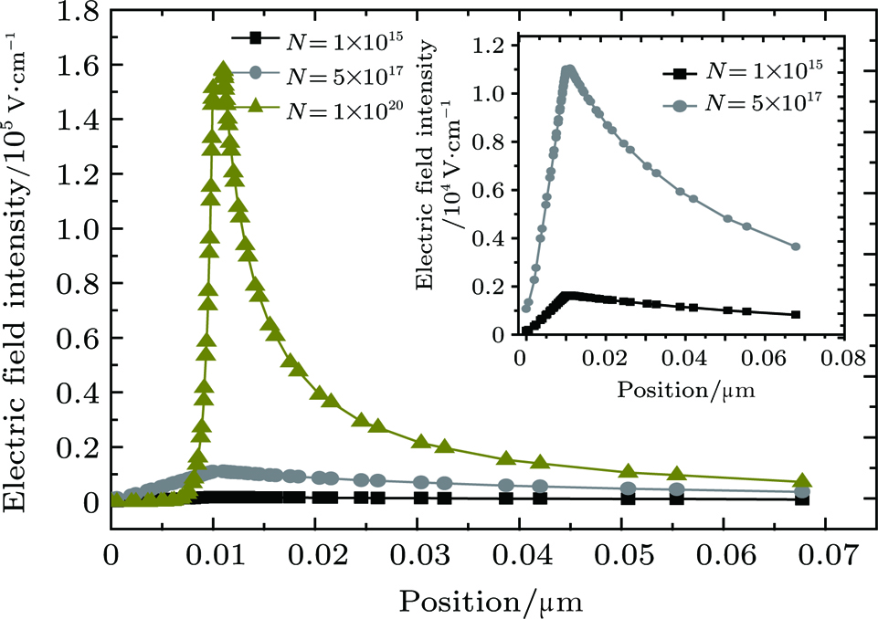
(color online) The electric field intensity in Y direction near front surface with different doping level of polycrystalline silicon layer. The position of