Progressive current degradation and breakdown behavior in GaN LEDs under high reverse bias stress
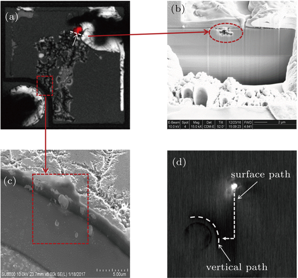
(color online) (a) Surface morphology of the GaN LEDs, (b) SEM images of the cross section after FIB cuts and (c) of the mesa side observed from a slight tile angle, and (d) OBIRCH image after breakdown failure.
