1. IntroductionFlexible electronics like solar cells and OLEDs have been studied intensively in recent years.[1,2] To improve device performance, contact resistance should be cut down to an acceptable extent, and this is usually achieved by silver-based conductive composites.[3–7] Right now, most of the conductive composites are made of silver particles. Due to the large sizes ( ) and irregular shapes of the particles, organic binders are usually added so as to make a sticky composite. Film is formed, and high temperature sintering (450–500 °C) is usually applied to as-prepared film to remove the organic additives, improving conductance.[8–10] However, the temperature is much higher than that most flexible plastic substrates (like polyethylene terephthalate, or PET) can bear, and in addition, higher temperature increases oxidation of the silver. Consequently, high-temperature curing should be avoided in flexible optoelectronics. Due to the fast development of flexible electronics, low-temperature-cured conductive composites are urgently needed. Silver nanowires (AgNWs) show excellent electrical conductivity. Transparent and conductive films based on AgNWs show sound optoelectronic performance of 90% (T%@550 nm), and
  /sq (sheet resistance,
  ).[11–13] Moreover, such performance can be achieved at low temperature (
 ).[14] It is anticipated that, by increasing the loading of nanowires, lower sheet resistance (
 /sq) could be obtained. Such film conductivity would be higher than that of the most commonly used transparent and conductive substrates like FTO (12–15 Ω/sq) and ITO (8–12 Ω/sq), and is appealing for optoelectronic devices.
During the last few years, AgNWs have been used to prepare flexible conductive composites. For example, Liou et al. prepared an embedded surface electrode with conductivity of 100 S/cm by mixing AgNWs and polyimide.[15] Xu et al. prepared a stretchable conductor with conductivity of 8.13×10³ S/cm using AgNWs as the conductive filler.[16] However, that conductivity is still lower than that of pristine silver (6.50×10⁵ S/cm). In order to further reduce the contact resistance of devices, film conductivity should be improved.
Therefore, in this work, a new conductive composite was prepared using AgNWs as the conductive filler and polyvinyl alcohol (PVA) as the binder. The composite was then used to prepare flexible conducting films at lower temperatures ( ). Effects of annealing temperature and duration, film thickness, and nanowire length on the conducting behavior of the conducting films were studied.[17] The films’ resistance to scratching, flexibility, and contact resistance were tested. Sheet resistance of 0.12 Ω/sq and conductivity of 2.63×10⁴ S/cm were obtained, which are better than comparable performance reported previously.[14,15] Moreover, Monte Carlo simulation was carried out to give more details of the film-conductivity effects brought about by varying nanowire length and nanowire density.[18,19]
2. Experimental detailsEthylene glycol (EG, 99.0%), silver nitrate (AgNO3, 99.8%), polyvinylpyrrolidone (PVP, MW  ), potassium chloride (KCl, 99.5%), nitric acid (HNO3, 65%), and polyvinyl alcohol (PVA, MW
  ) were all purchased from the domestic market and used as received. De-ionized water was made at our laboratory.
Silver nanowires were synthesized using a modified polyol method proposed by Xia et al.[20–22] First, a solution was prepared by dissolving PVP (2.36 g) and KCl (0.016 g) in EG (98 mL), and heated by an oil bath at 170 °C. Then, to trigger the reduction reaction, AgNO3 solution (0.07 mol/L, dissolved in EG, 50 mL) was introduced drop by drop during 5–10 min. The reaction was allowed to proceed for one hour, after which the resultant product was washed by ethanol and centrifuged 3–5 times, and then stored in de-ionized water by solvent exchange. To produce AgNWs with two different length distributions, we varied the rate of introducing the solution, the reaction temperature, and even the concentrations of reactants, as described in Refs. [21] and [22]. A conductive silver composite was prepared by mixing AgNWs and PVA as follows. A stock solution of PVA with concentration of ∼ 5 wt.% was prepared by dissolving PVA in de-ionized water at 95 °C. Then the stock solution was mixed with a AgNW suspension with volume ratio of 1:1.5, which gives a volume fraction of AgNWs of ∼ 50% in the dried composite.
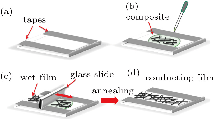
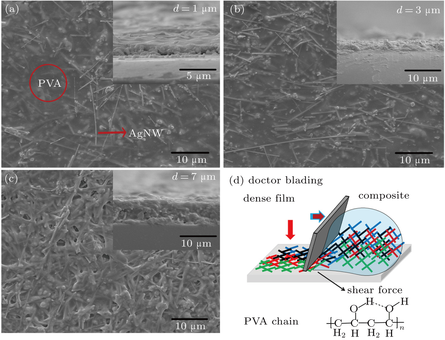
Films were coated using the doctor blading method reported in Refs. [23] and [24]. Glass slide and PET films were used as substrates, and before film coating, they were ultrasonically cleaned by acetone, de-ionized water, and ethanol, each for 10 min. Then conducting films were prepared as shown in Fig. 1. The as-coated wet film was dried at 100–150 °C for 0–60 min in the open air. In addition, samples with thicker films were prepared by repeating the coating process.
Crystallographic properties of AgNWs were characterized by x-ray diffraction (XRD, Bruker D8). The morphological property of AgNWs was monitored by scanning electron microscopy (SEM, Nova NanoSEM 230) with an acceleration voltage of 10 kV. The film thickness was tested by a profiler (Veeco Dektak 150). Sheet resistance of the as-fabricated films was tested by four-point probe measurement (SDY-4.5). Five different points were measured for each sample and an average was obtained. Contact resistance was evaluated by a digital source meter (Model 2400, Keithley). To evaluate the two key mechanical properties, coating resistance (against scratching) of the conductive films was evaluated by a pencil-plowing experiment,[25] while the flexibility (against deformation) was tested by measuring resistance to bending fatigue.[21]
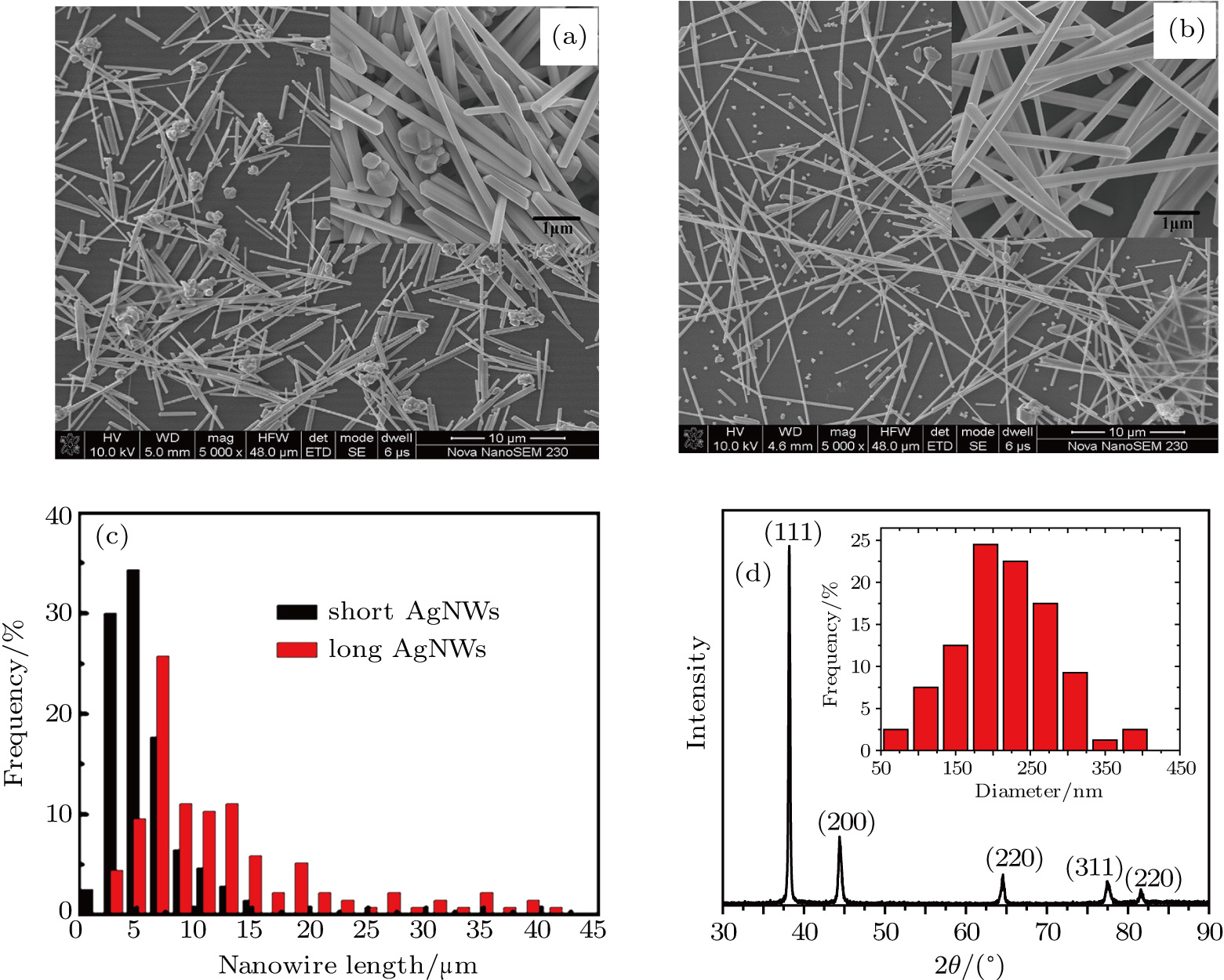
3. Results and discussion3.1. Surface morphological and crystallographic properties of AgNWsSEM surface morphology images of the as-synthesized AgNWs are shown in Figs. 2(a) and 2(b). Two different length distributions are shown in Figs. 2(c) and 2(d). For short AgNWs, the length is distributed mainly from  to
to  and centered at
  ; while for longer ones, the length is distributed mainly from
  to
to  and centered at around
  . In contrast, the distribution of the wire width is similar in the two cases. Besides nanowires, a few silver particles are present in the samples. These observations resemble those in Refs. [26] and [27]. On the other hand, XRD shows that these nanowires (and nanoparticles) are silver. As shown in Fig. 2(d), diffraction peaks at
  of 38.14°, 44.36°, 64.46°, and 77.46° can be associated to (111), (200), (220), and (311) planes of bulk silver (JCPDS file No. 04-0783). As will be described later, the length distribution plays an important role in the conducting behavior of these conducting films.
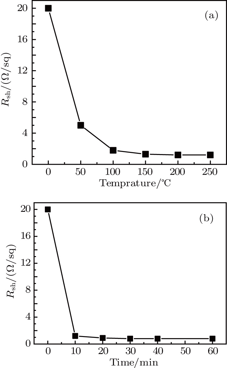
3.2. Effect of curing temperature, curing duration, film thickness, and nanowire length on conducting behavior of the conductive compositeIn order to evaluate the conductivity of AgNW based conductive composites, films were prepared and the effects of curing temperature and duration on the conduction of the films were examined. Figure 3 shows the variation of the sheet resistance  of the film with the annealing temperature and duration. It can be seen that higher temperature and longer period improve the film conductance. For the film that is only dried after coating,
  is 20 Ω/sq;
  decreases to 1.30 Ω/sq for the film annealed at 150 °C for 10 min but differs little for longer periods. On the other hand, when the annealing duration is fixed at 20 min, the film conductance is also maximized at annealing temperatures
  . As a result, annealing at 150 °C for 10 min is enough to maximize the film conductance. The variation in film conductance is attributed to the improved contact between nanowires, as will be discussed later.
Besides annealing processes, the film conductivity is also affected by the film thickness. For the sake of comparison, average volume resistivity ρ and average conductivity σ are deduced from sheet resistance  and film thickness d according to the following equation:[16]
 | |
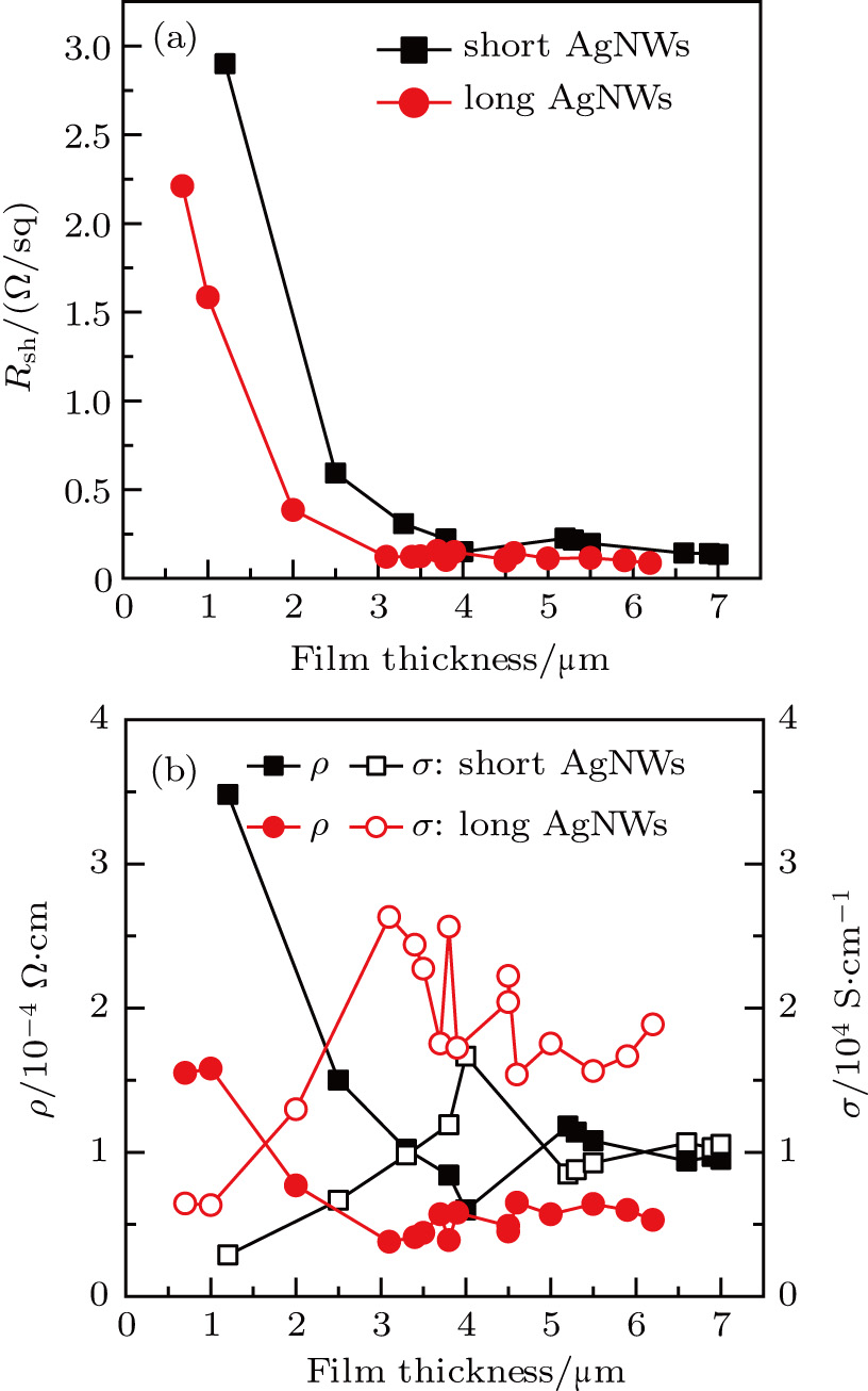
Then the effect of the film thickness on sheet resistance  , average volume resistivity ρ, and average conductivity are monitored; the results are shown in Fig. 4. It is observed that, for both long/short silver nanowires, sheet resistance
  of the conducting film decreases quickly at first, and then reaches its maximum. But for similar film thicknesses, longer nanowires show lower sheet resistance. The lowest sheet resistance is 0.12 Ω/sq for longer nanowires at the film thickness of
  , compared to 0.20 Ω/sq at the film thickness of
  for the shorter ones. Average resistivity ρ shows similar behavior, as can be seen in Fig. 4(b). With increasing film thickness, the film conductivity increases steeply at first, and then less steeply. The maximum conductivity is 2.63×10⁴ S/cm for longer AgNWs, but only 1.31×10⁴ S/cm for shorter ones. Both maxima are higher than those of carbon fiber reinforced plastics (CFRPs),[28–31] whereas the largest conductivity previously reported for stretchable conductors is 1–100 S/cm and 8.13×10³ S/cm.[16]
The film conductance is superior for three reasons: nanowire density, connection between nanowires, and nanowire length. First, as can be seen in Figs. 5(a)–5(c), the nanowire density increases with the film thickness. According to De et al., for AgNW based transparent and conducting films, increased nanowire loading or density can improve the film conductance.[32] Such effects can also be simulated, as will be discussed later. Second, the nanowires are surrounded by PVA chains in the films. While drying, the wet film becomes denser, which improves the connection between nanowires. On the other hand, as depicted in Fig. 5(d), “doctor blading” usually involves a shear force which causes nanowires to lie down on the surface; this is well reflected in our top view images. One can see that almost all the nanowires lie parallel with the substrate surface. Such alignment also contributes to the improved connection between nanowires. One more important reason is the addition of PVA. PVA is one of the main additives in water-based glues. According to the schematic inset in Fig. 5(d), hydroxyl groups are abundant in the PVA chains; such polar ligands tend to adhere to many materials due to the available hydrogen bonds. When the wet film dries, the PVA chains gel together, forming a dense matrix, which benefits the connection between nanowires. Also due to the assistance of PVA, sheet resistance of 0.75 Ω/sq and transparency of 86.9% were achieved by He et al. in AgNW based transparent and conductive networks.[33] Lastly, as stated with regard to transparent and conductive films, longer nanowires penetrate the network, helping to form a continuous unity, as suggested by Cui and coworkers.[34,35] By employing longer nanowires, the penetration can be much improved.[35] Such an effect has been well reflected in simulations.[36] A recent simulation done by our group shows that, at similar nanowire loadings, longer nanowires provide more conducting routes, producing better film conductance.[11]
3.3. Effect of nanowire length on film conductance revealed by Monte Carlo simulationTo learn more about the effects of the nanowire density and nanowire length on the film conductance, a Monte Carlo based simulation was carried out similar to that done before.[11] Briefly, a 2D square random network was generated by nanowires with length/width distributions similar to the experimental samples (as shown in Fig. 2). Since two different length distributions were obtained, two kinds of 2D networks were generated. To increase the nanowire density, the area fraction of nanowires was increased. The sheet resistance of the network was calculated by a strategy of equivalent circuit transformation, the details of which will be described in another separate work. To find the relationship between the film conductivity and the topological properties of the network, the lengths of the conducting routes were calculated, along with the sheet resistance, as shown in the schematic of Fig. 6(a). In order to make a meaningful comparison, the length ratios of the conducting routes were calculated for both length distributions, while the contact resistance between nanowires was not considered. Then the effect of the nanowire density and nanowire length on both the length ratio and sheet resistance was obtained. As shown in Fig. 6(b), in both distributions, with increasing area fraction, the length ratio of the conducting routes increases, while the sheet resistance decreases. But with area fraction held constant, longer nanowires yield larger length ratios and lower sheet resistance. Such behavior clearly shows that the length ratio is important in determining the film conductance. For homogeneous networks, a higher length ratio of conducting routes benefits film conductivity. The mechanism will be discussed in greater detail in another work.
3.4. Application of AgNW based conductive compositeIn order to show the potential application of a highly conductive silver composite in flexible optoelectronics, three related properties were examined for conducting films made from the composite: (i) resistance to scratching, (ii) flexibility, and (iii) contact resistance between the film and a transparent & conductive substrate.
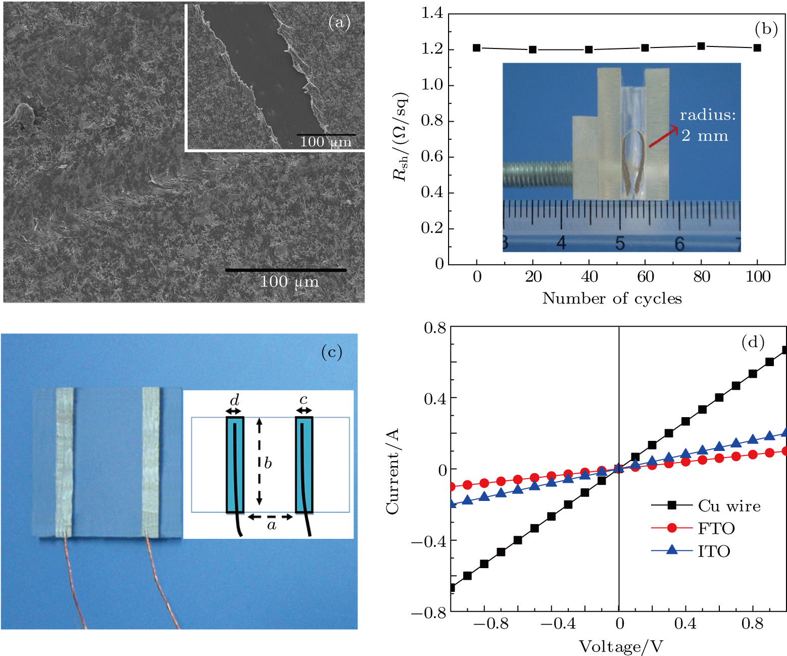
The first aspect was evaluated by a pencil-plow experiment, as shown in Fig. 7(a). The resistance of the film coating to scratching was measured to be 6H for film thickness of  . The superior resistance is due to the addition of PVA. It is well known that hydroxyl groups are abundant on PVA molecular chains (Fig. 5(d)); thus hydrogen bonds could appear between these polar ligands. Meanwhile, a condensation reaction could occur between these ligands, both helping to form a compact matrix, which benefits adhesion of film on the substrate. On the other hand, our comparison between films at thicknesses of
  and
and  found that the film thickness is also a key parameter for the film’s scratch resistance. It is related to the relative hardness of AgNWs and also the nanowire density in the films. It is well known that the relative hardness of metallic silver is higher than that of graphite used in pencils. Concretely, Mohs hardness of metallic silver is 2.5–3, but 1.5 for graphite.[37] It would be easier to obtain more homogeneous film along with higher nanowire density at greater thickness; thus the scratch resistance could be much improved by increasing the film thickness.
The second aspect, flexibility, was evaluated by monitoring the variation of bending fatigue resistance of the conducting film. As shown in Fig. 7(b), even when a sample is bent at curvature radius of 2 mm for 100 cycles, sheet resistance  hardly changes. Such flexibility is also due to the addition of PVA. On the other hand, AgNWs themselves show excellent flexibility, as has been reported often.[14,20]
Finally, the contact resistance was measured as illustrated in Fig. 7(c). Resistance of Cu/AgNW composite/FTO(ITO)/AgNW composite/Cu ( ) consists of three parts: contact resistance between Cu wires and the electrodes of the digital source meter (
 ), sheet resistance of the substrate between the two parallel conductive composite films (
 ), and contact resistance of the interface Cu/AgNW composite/FTO(or ITO) (
 ). The contact resistance at the electrodes was first evaluated to be 1.4 Ω.
  is calculated as follows:
By measuring the dimensions of a and b,  for FTO and ITO was estimated to be 6.0 Ω and 3.4 Ω, respectively. So the resistance of the whole system of Cu/AgNW composite/FTO (or ITO)/AgNW composite/Cu was calculated by fitting the I–V curves. Then contact resistance
  of interface Cu/AgNWs composite/FTO (or ITO) was calculated according to
The results are collected in Table 1.
Table 1.
Table 1.
 Table 1.
Electric and geometric parameters collected from evaluation of current–voltage behavior of interface between conductive composite and substrates.
.
| Sub-strate |
(a/b/c/d)/cm |
Rsh/(Ω/sq) |
Rsub/Ω |
Relect/Ω |
Rwhole/Ω |
Rcont/Ω |

|
| ITO |
0.6/1.4/0.4/0.4 |
8.0 |
3.4 |
1.4 |
5.9 |
1.1 |
1.0 |
| FTO |
1.2/2.5/0.25/0.3 |
12.4 |
6.0 |
1.4 |
11 |
3.6 |
2.6 |
| Table 1.
Electric and geometric parameters collected from evaluation of current–voltage behavior of interface between conductive composite and substrates.
. |
Then, the contact resistance for FTO and ITO was calculated to be 2.6 Ω/cm2 and 1.0 Ω/cm2, respectively. The larger value for FTO is due to the higher sheet resistance, because the contacting resistance of the interface of Cu/AgNWs composite/FTO(or ITO) also contains part of the substrate (FTO/ITO). Finally, the high scratch resistance of the film, high flexibility, and low contact resistance make such films suitable for applications in optoelectronic devices.


