Electronic structure and nematic phase transition in superconducting multiple-layer FeSe films grown by pulsed laser deposition method
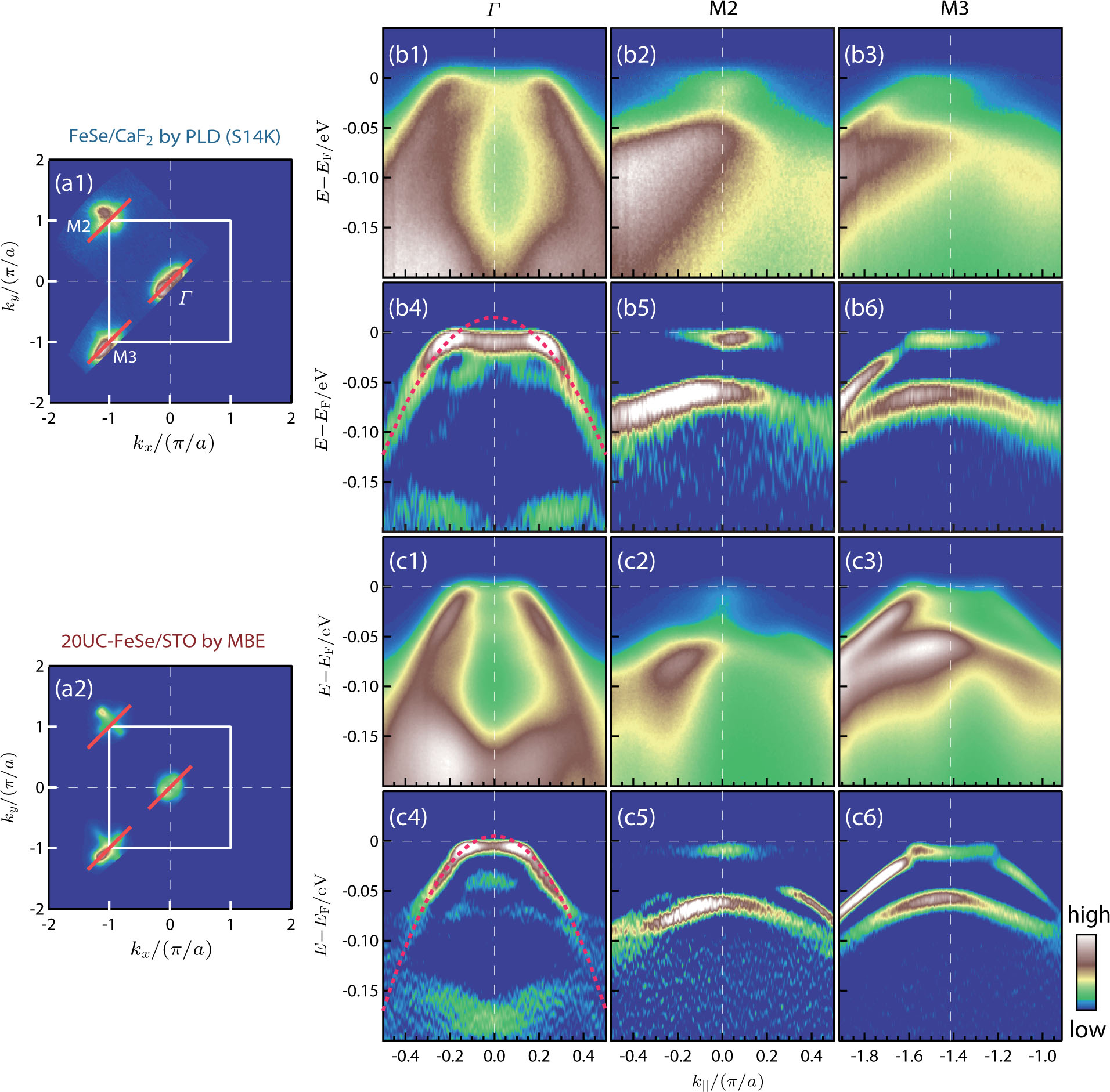
Comparison of electronic structure between the PLD-grown multiple-layer FeSe/CaF2 film and the MBE-grown 20-layer FeSe/SrTiO3 film. (a1) and (a2) show Fermi surface mapping of the PLD-grown S14K sample and MBE-grown 20-layer film, respectively, measured at 30 K. (b1)–(b3) show original data of the band structure for PLD-grown S14K sample measured along three momentum cuts. The locations of the momentum cuts are marked in (a1) by red line. (b4)–(b6) show corresponding second derivative images with respect to energy corresponding to (b1)–(b3). (c1)–(c3) represent original data of band structure measured along the three momentum cuts; their corresponding second derivative images are shown in (c4)–(c6).