Coherent charge transport in ferromagnet/semiconductor nanowire/ferromagnet double barrier junctions with the interplay of Rashba spin–orbit coupling, induced superconducting pair potential, and external magnetic field
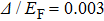
(color online) Illustration of zero-bias conductance peak in the cases that the strength of the external magnetic field exceeds the critical value