Coherent charge transport in ferromagnet/semiconductor nanowire/ferromagnet double barrier junctions with the interplay of Rashba spin–orbit coupling, induced superconducting pair potential, and external magnetic field
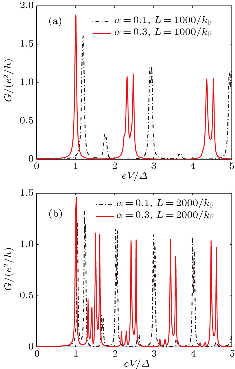
(color online) The charge conductance as a function of the bias voltage for two different thicknesses of the semiconductor nanowire: (a)