Spectral dynamical behavior in two-section, quantum well, mode-locked laser at 1.064 μm
Wei Si-Hang1, 2, Ma Ben1, 2, Chen Ze-Sheng1, 2, Liao Yong-Ping1, 2, Hao Hong-Yue1, 2, Zhang Yu1, 2, Ni Hai-Qiao1, 2, †, Niu Zhi-Chuan1, 2, ‡
State Key Laboratory for Superlattices and Microstructures, Institute of Semiconductors, Chinese Academy of Sciences, Beijing 100083, China
Synergetic Innovation Center of Quantum Information and Quantum Physics, University of Science and Technology of China, Hefei 230026, China


† Corresponding author. E-mail: nihq@semi.ac.cn zcniu@semi.ac.cn

Project supported by the National Basic Research Program of China (Grant Nos.~2013CB933304 and 2012CB932701), the National Natural Science Foundation of China (Grant Nos. 61274125 and 61435012), and the Strategic Priority Research Program (B) of the Chinese Academy of Sciences (Grant No. XDB01010200).

Abstract

In this study, two-section mode-locked semiconductor lasers with different numbers of quantum wells and different types of waveguide structures are made. Their ultrashort pulse features are presented. The spectral dynamical behaviors in these lasers are studied in detail. In the simulation part, a two-band compressive-strained quantum well (QW) model is used to study thermally induced band-edge detuning in the amplifier and saturable absorber (SA). A sudden blue shift in laser spectrum is expected by calculating the peak of the net gain. In the experiment part, the sudden blue shift in the emission spectrum is observed in triple QW samples under certain operating conditions but remains absent in single QW samples. Experimental results reveal that blue shift phenomenon is connected with the difference between currents in two sections. Additionally, a threshold current ratio for blue-shift is also demonstrated.

1. Introduction

There is an increasing interest in nonlinear optical physics when continuous-wave (CW) pump sources are replaced by ultrafast mode-locked lasers, especially in quantum optics.[1,2] Utilizing ultrashort and ultrafast laser pulses in spontaneous parametric down-conversion (SPDC) and optical frequency conversion is not only showing advantages in lab experiments, but also displaying potentials in integrated quantum information applications.[3,4] Usually such high-energy optical pulses are offered by large optical equipment,[5,6] however it can be replaced by semiconductor laser diodes (LD) if nonlinear materials like PPLN with large secondary nonlinear factor are used.[7] Furthermore, in the quantum optics field where pump pulses with less power and more speed are desired,[8] monolithically fabricated semiconductor mode-locked laser capable of operating at GHz speed[9,10] becomes a promising candidate. With compact structure and low cost, it is also desired in other applications including noninvasive biological imaging,[11] data communication, optical clocking, high-speed optical sampling, all-optical clock recovery, and microscopy.[12,13]

Researchers have been investigating two-section mode-locked lasers for years. Several optimized structures[14,15] and the corresponding models have been developed.[16,17] Recently, mode-locked regimes, noise characteristics, pulse widths, and output powers of these monolithically fabricated lasers have been studied and demonstrated in detail.[18,19] However, as an imperative parameter in frequency conversion, emission spectrum is less mentioned and modeled. A few excellent works show that band-edge detuning in two sections is accountable for the unique spectrum characteristics of these LDs.[20,21] In these works, by taking the absorber as a low pass filter, an easy way to understand spectral dynamical behaviors in similar two-section structures is achieved.[22] As wavelength characteristics around threshold current have already been studied in detail, in this paper a spectrum far above threshold current is modeled and tested. Experiment results are demonstrated in Sections 3 and 4, and further explanations with a simple model can be found in Section 2.

2. Theory

Practically, the active layers of two sections are the same materials because the laser diodes are made from one single wafer. Therefore, considering null electrical and thermal interactions between two sections, it is reasonable to discuss them with the same two-band compressive-strained quantum well model.[23] Parameters are shown in Table 1.

During the simulation, a single compressed 6 nm InGa As quantum well with optical conversion between first conduction band and first heavy hole band is considered. Gain spectrum and absorption spectrum of two sections are obtained by gain function[24]

The parameters in two-band compressive-strained quantum well model.

Symbol Value(InAs) Value(GaAs) Units Meaning
d 6.0584 5.6533 Å crystal distance
8.329 11.88 N/cm elastic stiffness
4.526 5.38 N/cm elastic stiffness
a –6.0 –9.77 eV deformation potential
b –1.8 –1.7 eV deformation potential
20.4 6.85 Luttinger constant
8.3 2.1 Luttinger constant
mc 0.023 0.067 conduction band electron mass
valence band heavy hole mass on growth plane
valence band heavy hole mass vertical to growth plane
where is photon energy, is electron mass, is vacuum permittivity, is electron charge, is material refractive index, is group index, is momentum matrix element, is reduced density, is quantum well band gap energy, is energy of eigenstates, is carrier relaxation time,[25] and are the probabilities of the conduction and valence band energy level being occupied by electrons and holes. Group index is interpreted as
where is the mode effective index.

Normally, the emission wavelength of an operating laser diode is corresponding to the peak of its net gain spectrum. The situation is more complicated in two-segment lasers, where net gain spectrum can be manipulated by its modulation section. Therefore it is necessary to analyze the gain spectrum of the amplifying section and the absorption spectrum of absorber section simultaneously. The temperature dependence of InGaAs band gap reads[26]

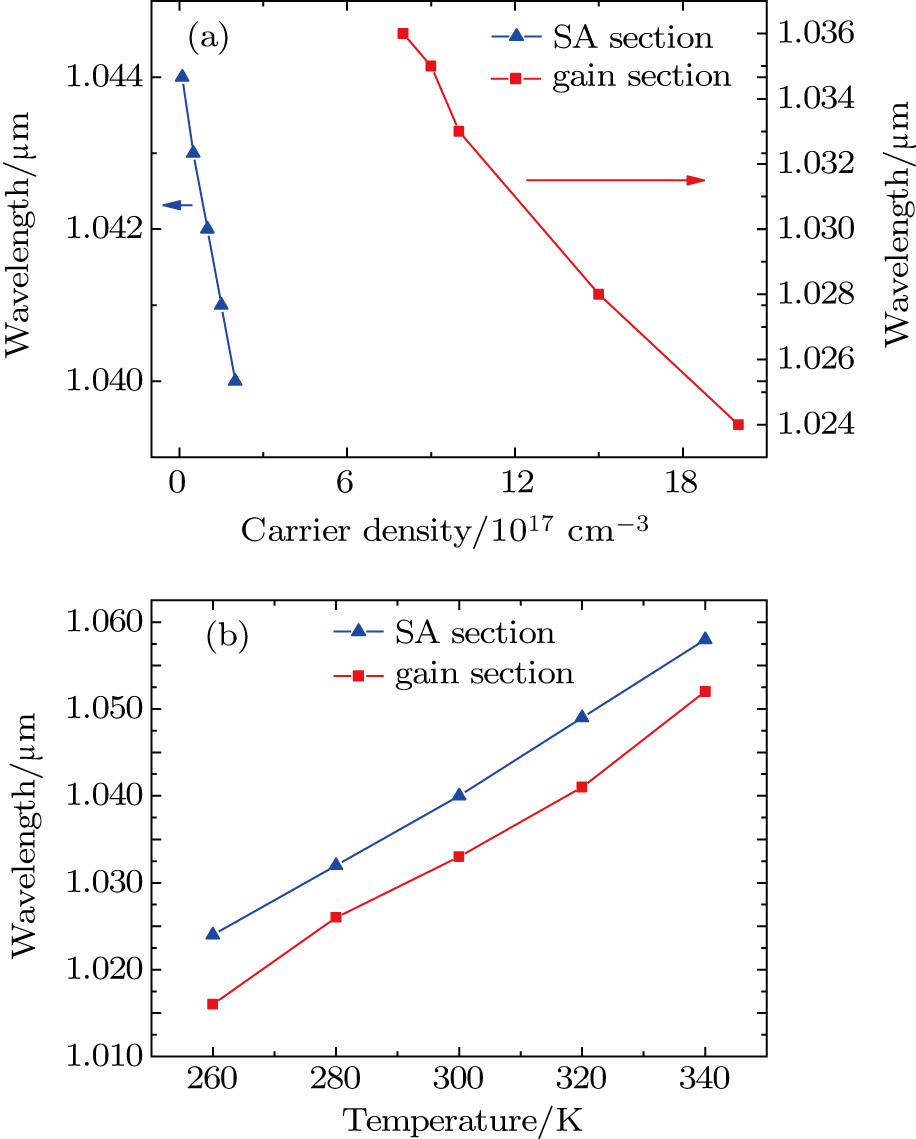
Figure 1(a) shows the calculated gain peaks and absorption edges with different carrier densities at 300 K. The slopes are −0.5 nm/10 and −0.24 nm/10, respectively. A different scenario occurs in Fig. 1(b) when carrier density remains constant while temperature is varied. The average rates are 0.425 nm/K and 0.41 nm/K, respectively. From the simulated results, we can find that gain peak and absorption edge red-shift with temperature and blue-shift with carrier density. For two-section mode-locked lasers operating at a large injection current and a nearly depleted absorber, carrier densities of the active layer in both sections are hardly changed. In this case, the thermal drift of the bandgap is substantially more involved.[27] Therefore temperature-induced dynamical behaviors are first considered when wavelength features are discussed.

Fig. 1. (color online) (a) Gain peaks of gain section (red squares) and absorption band-edges of saturable absorber (SA) (blue triangles) against carrier density in quantum well region. (b) Gain peaks and absorption band-edges against temperature of quantum well region.

Temperature rising depends on the heat generated by Joule effect,[28] which is proportional to products. It can be expressed in the form

where and are the factors of heat generation and dissipation in quantum well region in each section. and are the temperature risings in each section. and are the factors of total temperature rising proportional to . The first subscripts a and g represent saturable absorber (SA) and gain, and the second subscripts g and d represent generation and dissipation. Temperature difference between sections is presented (note that in laser diode is hardly changed with above threshold current)[29] as
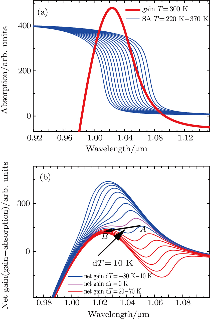
The above equation gives the connection between and . Considering the practical geometry of the two-section mode-locked laser with large gain-to-SA ratio, amplitudes of gain and absorption spectrum are modified before depicted in Fig. 2(a). Net gain spectrum calculated according to Fig. 2(a) is illustrated in Fig. 2(b). A sudden blue shift from A point to B point is observed when surpasses a value (10 K in this case). This sudden blue shift is enough to overcome the thermal red shift in LDs, therefore this blue shift is assumed to be observed in the experiment. However, current ratio should exceed a threshold (larger than ) to achieve blue shift according to Eq. (7).

Fig. 2. (color online) (a) Gain spectrum (red line) at 300 K and absorption spectrum (blue lines) when SA temperature increases from 220 K to 370 K with 10 K interval. (b) The corresponding net gain spectrum when ranges from −80 K to 70 K. The arrow indicates the onset of blue shift. is from Eq. (7).
3. Experiment of 1QW laser structure

In the experiment, two-section lasers designed based on the above model were grown by MBE on 2 degree off-cut Si-doped GaAs substrates. The active region of the laser structure was a 6 nm thick compressed InGaAs quantum well buried in the middle of 40 nm GaAs barrier, with two 200 nm undoped GaAs waveguide layers and two 1400 nm highly-doped AlGaAs cladding layers on both sides of it for optical and electrical confinements. All layers were grown at 873 K except the thin InGaAs quantum well layer which was grown at 773 K.

After single QW sample 16A was grown, the wafer was processed into a laser chip with 4.5 μm wide and 2.1 mm long ridge waveguide structure. The 2.1 mm long cavity was separated by a 2000 μm gain section, a 70 μm absorber section, and a 40 μm passive section through conventional chemical etching techniques. A processed wafer was cleaved with both facets uncoated and soldered to the copper heat-sink for testing. The pulse widths, radio frequency (RF) signals, and optical characteristic measurements were carried out by APE intensity autocorrelater (IAC), 50 GHz radio frequency (RF) analyzer, optical spectrum analyzer (OSA), and Fourier transform infrared spectroscopy (FTIR) after laser output was coupled to a 3-meter long single mode fiber. During the experiment the heat sink temperature was set to 20 °C.

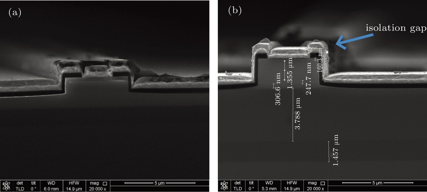
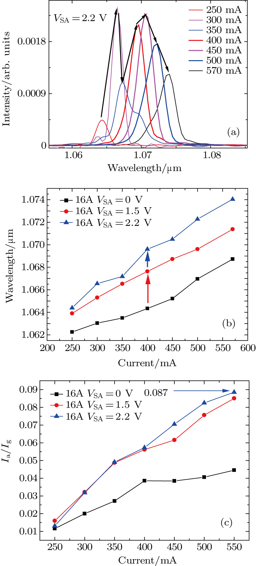
The scanning electron microscope (SEM) image of 16A is shown in Fig. 3. During the experiment, we sweep injection current under certain reverse bias to record maximum and minimum current point when RF signal analyzer shows over 20 dB signal-to-noise ratio (SNR). Then we randomly pick a current point within the range for following spectrum and pulse test. Figure 4 shows that mode locking starts with minimum injection current 300 mA under 2.4 V reverse bias and ends with maximum injection current 700 mA under 1.5 V reverse bias. RF signal with 30 dB SNR shown in Fig. 5 is tested by IAC. The IAC trace is fitted with function before being inserted into Fig. 4. Although it shows a wider pulse width than usually reported, on one hand because of the narrow gain spectrum provided by single InGaAs QW, on the other hand because of the pulse broadening effect brought by gain dispersion and self-phase modulation,[30] ultrashort and ultrafast output signal is obtained with this two-section 1.064 μm single QW laser diode. The emission wavelength is measured when reverse bias is enough for mode locking. Figure 6(b) shows the wavelength characteristics against injection current under distinctive reverse biases. It indicates that wavelength red shifts with both injection current and reverse bias. The red shift with increasing injection current can be explained by Joule effect in the gain section.[31] The red shift with reverse bias can be explained by a combined result of Starks effect[32,33] and a slightly increased by the enhanced absorption. Additionally, although the device is tested under enough reverse bias for mode locking, no sign of blue shift is observed. Currents of the absorber and amplifier are recorded simultaneously with spectrum of 16A by direct current (DC) sources and FTIR. The current ratio between these sections is calculated and shown in Fig. 6(c). In order to match with the model in Section 2, the following analysis is limited to the regimes far beyond threshold current. Within this current range, ratio increases with injection current and finally saturates at 550 mA. The maximum ratio is 0.087 under 2.2 V reverse bias. Such small ratio is assumed insufficient to obtain enough for blue shifting.

Fig. 3. (color online) Scanning electron microscope (SEM) image of cross section of 16A (a) and 23A (b). The isolation gap can be seen in 23A.
Fig. 4. (color online) The mode locking points (green triangles) selected by RF analyzer. The inset shows the ICA trace and its fitting curve when injection current is 500 mA and reverse bias is 2.2 V.
Fig. 5. RF spectrum shows a 17.3 GHz fundamental frequency signal at 500 mA injection current and 2.2 V reverse bias.
Fig. 6. (color online) (a) Spectrum of 16A under 2.2 V reverse bias. The black arrows show the wavelength change direction. (b) Wavelength with the increasing injection current under 0 V, 1.5 V, and 2.2 V reverse biases for 16A. (c) Measured current ratio of two sections under 0 V, 1.5 V, and 2.2 V reverse biases.
4. Experiment of 3QW laser structure

The small current generated in the absorber of 16A was partly due to the thin active layer as well as the small optical confinement and partly due to the short absorber length. In order to achieve blue shift, we modified the absorber structure to manipulate the current generated in it. Three quantum wells laser samples were carefully designed and grown. Samples 10A and 10B were made from the same wafer, which had the similar epilayer structure as 16A except three 6 nm quantum wells in the middle. Sample 23A was similar to 10A and 10B except that two 200 nm GaAs waveguide layers were replaced by a 3000 nm AlGaAs layer. The wafers above were processed into a laser diode. Three samples were made during fabrication, sample 10A with 2000 μm gain section, 70 μm absorber section, and 40 μm passive section, sample 10B with 1770 μm gain section, 300 μm absorber section, and 40 μm passive section, sample 23A with 1770 μm gain section, 300 μm absorber section, and 40 μm passive section. They were cleaved to diodes with both facets uncoated and tested under the same condition as 16A.

The SEM image of 23A is also shown in Fig. 3. Mode-locked regimes of three samples are shown in Fig. 7. Normally optimized two-section mode-locked lasers have a similar configuration to 10A, which possess a nearly 3.5% absorber-to-gain ratio to give the narrowest pulse with minimum noise.[15] In our case, 5.3 ps pulse is achieved and depicted in the first inset. Sample 10B with longer absorber section is designed to achieve larger generated photo-current by enhanced absorption. Sample 23A with larger AlGaAs waveguide layer is designed to achieve smaller photo-current by reduced optical density[34] in the active area. These samples are subsequently tested. ICA traces with sech fitting curves of 10B and 23A are also inserted into the figure. Their reverse biases range from 0.3 V to 0.9 V and from 0.9 V to 1.9 V, respectively.

Fig. 7. (color online) The stable mode locking points of 10A (red squares), 10B (blue triangles), and 23A sample (black dots). The insets show that pulse width of 5.3 ps, 4 ps, and 14.6 ps are obtained from 10A, 23A, and 10B under (200 mA, V), (400 mA, −1.5 V), and (620 mA, −0.9 V), respectively.

The first clue of enhanced absorption in 10B is that the reverse bias of 10B drops considerably from around 2 V to below 1 V compared with 10A when LD is mode-locked. For 23A which has less optical confinement than 10B and longer absorber length than 10A, the reverse bias is between 10A and 10B. Therefore the absorption of the absorber section increases with its length and decreases with its optical confinement. Spectrum and current measurements for each sample are carried out in the same way. Results of 10A and 10B are shown in Fig. 8(d). SA of 10A is subjected to different reverse biases of 0.9 V, 1.5 V, and 2 V during the test. In the experiment, as soon as reverse bias reaches 1.5 V, the emission wavelength of 10A no longer monotonously red shifts with current. A clear blue shift can be observed. The mechanism in Section 2 is demonstrated by a wavelength jump of nearly 2 nm between 100 mA and 200 mA. This wavelength change along with another blue shift of nearly 4 nm under 2 V reverse bias indicates that current ratio should surpass threshold within this current range. To further investigate the absorber length influence on spectral dynamical behavior, 10B is subsequently tested. In Fig. 8(d), 10B shows a significant blue shift over 10 nm at 400 mA injection current and 0.9 V reverse bias.

Fig. 8. (color online) Spectrums of 10A under 1.5 V (a) and 2 V (b) reverse bias, and the spectrum of 10B under 0.9 V (c) reverse bias. The black arrows show the wavelength changes direction when injection current increases. (d) Emission wavelengths of 10A and 10B with the increasing injection current under 0 V, 0.9 V, 1.5 V, 2 V reverse biases and 0 V, 0.9 V reverse biases, respectively. (e) Calculated ratio for 10A. The red thick line indicates blue shift. (f) Calculated ratio for 10B. The red thick line indicates blue shift.

Current ratio of 10A is concluded in Fig. 8(e). increases with injection current and finally saturates around 300 mA similar to the discussion of 16A, however the maximum value is substantially bigger. The maximum points shown in Fig. 8(e) are 0.131, 0.199, and 0.247 under 0.9 V, 1.5 V, and 2 V reverse biases. Blue shift only occurs in 1.5 V and 2 V cases indicates that 0.131 is still below the threshold . Therefore, considering the similar configuration of two samples, it is reasonable to assume 0.087 is also below threshold of 16A.

Current ratio of 10B is illustrated in Fig. 8(f). The increases with injection current and saturates at 400 mA with a maximum value of 0.353. For 10A, threshold is smaller than maximum value 0.199 because blue shift occurs before reaches maximum. For 10B, the threshold is almost equal to maximum value 0.353. The threshold difference between 10A and 10B can be explained by the difference between their SA lengths. in Eqs. (4)–(6), which is associated with the electrical to optical power conversion efficiency, is not directly related to the length of sections.[35] However is closely related to the contact area.[36] Therefore threshold can be interpreted as

of 10B is over 4 times as large as that of 10A, therefore threshold of 10B should be larger than 10A.

Single quantum well sample 16A has less optical confinement than multiple quantum well samples 10A, and therefore we cannot distinguish the influence of quantum well numbers and optical confinement on . In order to test the influence of optical confinement on spectral dynamic behavior alone, sample 23A is compared with 10B. Figure 9(b) illustrates the output wavelength as a function of injection current under different reverse biases. A sudden blue shift at 1.5 V reverse bias can be observed. The blue shift in sample 23A has a larger reverse bias compared with 10B due to the decreased absorption. Current ratio of 23A is given in Fig. 9(c). On one hand, large threshold around 0.27 is comparable to the ratio in 10B as expected for long SA device. On the other hand, it decreases from over 0.3 to 0.27 because of the reduced optical confinement. All samples above are measured within the range where they can mode lock but not all of them show wavelength jump phenomenon. is an important parameter to explain spectral behavior. From the experimental result, it is obvious that blue shift is connected with the difference between current ratio and threshold ratio . When is below , no sudden blue shift is observed, whereas larger blue shift occurs if is above . The numbers of quantum wells, length of SA section, and optical confinement are both assumed to affect the threshold ratio. This phenomenon has been clarified by the model discussed in Section 2, which demonstrates that spectral features are largely controlled by thermally induced band gap detuning between two sections.

Fig. 9. (color online) (a) Spectrum of 16A under 2.2 V reverse bias. The black arrows show the wavelength change direction when injection current increases. (b) Emission wavelength with the increasing injection current under 0 V, 0.9 V, and 1.5 V reverse biases for 23A. (c) Measured ratio for 23A. The red thick line indicates blue shift.
5. Conclusion

In summary, InGaAs/GaAs based quantum well lasers with four distinctive structures are made and ultrafast output pulses below 10 ps around 1.064 μm are obtained. Output wavelength shows constant red shift in single quantum well samples and sudden blue shift in three quantum wells samples. A model to clarify the phenomenon is made. During the experiments, blue shift shows a direct connection with the current ratio in two sections. Thermally induced band gap shifts of two sections are accountable for this sudden blue shift. The threshold ratio for blue shift increases with absorber length and decreases with optical confinement. Furthermore, wavelength jump and mode locking are not necessarily connected from the above point of view. Samples of one quantum well and three quantum wells showing different spectral dynamical behaviors are both successfully mode locked. However, the influence of thermal band-edge detuning on quality of mode locking in two-section mode-locked lasers should not be overlooked.

Reference
[1] Ma X S Zotter S Kofler J Jennewein T Zeilinger A 2011 Phys. Rev. 83 043814
[2] Pelc J S Yu L De Greve K McMahon P L Natarajan C M Esfandyarpour V Maier S Schneider C Kamp M Höfling S Hadfield R H Forchel A Yamamoto Y Fejer M M 2012 Opt. Express 20 27510
[3] Collins M J Xiong C Rey I H Vo T D He J Shahnia S Reardon C Krauss T F Steel M J Clark A S Eggleton B J 2013 Nat. Commun. 4 2582
[4] De Greve K Yu L McMahon P L Pelc J S Natarajan C M Kim N Y Abe E Maier S Schneider C Kamp M Höfling S Hadfield R H Forchel A Fejer M M Yamamoto Y 2012 Nature 491 421
[5] Peng Y Wang Z Li D Zhu J Wei Z 2016 Chin. Phys. 25 054205
[6] Lin B Zhang Q L Zhang D X Feng B H He J L Zhang J Y 2016 Chin. Phys. Lett. 33 074203
[7] McMillan A R Labonte L Clark A S Bell B Alibart O Martin A Wadsworth W J Tanzilli S Rarity J G 2013 Sci. Rep. 3 2032
[8] Ngah L A Alibart O Labonte L D’Auria V Tanzilli S 2015 Laser Photonics Rev. 9 L1
[9] Lianping H Stolarz P Dylewicz R et al. 2010 IEEE Photonic. Tech. L. 22 727
[10] Liu S T Zhang R K Lu D Kan Q Wang W Ji C 2016 Chin. Phys. Lett. 33 064205
[11] Moreaux L Sandre O Charpak S Blanchard-Desce M Mertz J 2001 Biophys. J. 80 1568
[12] Avrutin E A Marsh J H Portnoi E L 2000 IEE P-Optoelectron. 147 251
[13] Kaiser R Huettl B 2007 IEEE J. Sel. Top. Quant. 13 125
[14] Camacho F Avrutin E A Cusumano P Helmy A S Bryce A C Marsh J H 1997 IEEE Photonic. Tech. 9 1208
[15] Stolarz P M Pusino V Akbar J et al. 2015 IEEE J. Sel. Top. Quant. 21 1
[16] Otto C Luedge K Vladimirov A G Wolfrum M Schoell E 2012 New J. Phys. 14 1
[17] Vladimirov A G Turaev D 2005 Phys. Rev. 72 033808
[18] Akbar J Hou L Haji M Strain M J Marsh J H Catrina B A Kelly A E 2012 Opt. Lett. 37 344
[19] Thompson M G Rae A R Xia M Penty R V White I H 2009 IEEE J. Sel. Top. Quant. 15 661
[20] Javaloyes J Balle S Avrutin E A et al. 2013 International Conference on Transparent Optical Networks IEEE 2013 Cartagena, Spain 1
[21] Javaloyes J Balle S 2010 IEEE J. Quantum Elect. 46 1023
[22] Stolarz P M Javaloyes J Mezosi G et al. 2011 IEEE Photonics J. 3 1067
[23] Chuang S L 1991 Phys. Rev. 43 9649
[24] Zhang P Song Y Tian J Zhang X Zhang Z 2009 J. Appl. Phys. 105 053103
[25] Hunsche S Leo K Kurz H Köhler K 1994 Phys. Rev. 50 5791
[26] Botha J R Leitch A W R 2000 J. Electron. Mater. 29 1362
[27] Javaloyes J Balle S 2012 IEEE J. Quantum Elect. 48 1519
[28] Jae-Ho H Park S W 2004 IEEE T. Device Mat. Re. 4 292
[29] Crump P Erbert G Wenzel H Frevert C et al. 2013 IEEE J. Sel. Top. Quant. 19 1501211
[30] Agrawal G P 1991 IEEE J. Quantum Elect. 27 1843
[31] Li S G Gong Q Cao C F Wang X Z Yan J Y Wang H Y 2015 Chin. Phys. Lett. 32 75
[32] Kuo Y H Lee Y K Ge Y Ren S Roth J E Kamins T I Miller D A B Harris J S 2005 Nature 437 1334
[33] Chemla D S Damen T C Gossard A C Wiegmann W Wood T H Burrus C A 1985 Phys. Rev. 32 1060
[34] Fan J Zhu L Dogan M Jacob J 2014 Opt. Express 22 17666
[35] Piprek J Abraham P Bowers J E 1999 IEEE J. Sel. Top. Quant. 5 643
[36] Karim A 2004 8th International Multitopic Conference December 24–26, 2004 Lahore, Pakistan 659 10.1109/2944.788430