† Corresponding author. E-mail:
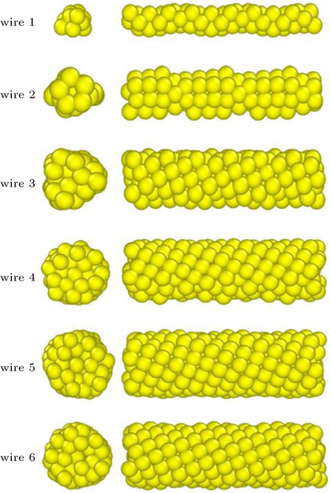
Lead nanowire occupies a very important position in an electronic device. In this study, a genetic algorithm (GA) method has been used to simulate the Pb nanowire. The result shows that Pb nanowires are a multishell cylinder. Each shell consists of atomic rows wound up helically side by side. The quantum electron transport properties of these structures are calculated based on the non-equilibrium Green function (NEGF) combined with the density functional theory (DFT), which indicate that electronic transport ability increases gradually with the atomic number increase. In addition, the thickest nanowire shows excellent electron transport performance. It possesses great transmission at the Fermi level due to the strongest delocalization of the electronic state. The results provide valuable information on the relationship between the transport properties of nanowires and their diameter.
In the last two decades, nanowires have been a focus of material science and the condensed matter physics, because metallic nanowires display an interesting quantum phenomenon that may be exploited to generate new-generation electronic device. Lead has been applied in many parts of devices, because it is widespread, soft, dense, ductile, easy to extract, and highly malleable metal with poor conductivity.[1] Pb nanowire is superconducting and superconducting nanodevices are predominately prepared or fabricated on semiconductor substrates.[2] A great deal of progress has been made in studying the metallic nanowire and its fabricating method. For example, Yang et al.[3] reported a one-step methodology for the fabrication of highly conductive and stretchable Ag nanowires composite electrodes based on a high-intensity pulsed light (HIPL) technique. Repetto[4] fabricated the aluminum nanowire electrodes by defocused ion beam sputtering. Volosskiy et al.[5] obtained ultrathin metallic nanowires by a metal-organic framework template. These advances are very valuable to learn about the fabricating method of this kind of metallic nanowire, but they do not focus on their properties. On the nanoscale, study of the properties of nanowires is valuable because it is important for potential applications in the fields of electronics, magnetic medium, optics, thermoelectronic, sensor devices, and creating a new generation of electronic devices.[6–13] Tang et al.[10] adopted in-tandem in situ TEM and molecular dynamics (MD) simulations in order to investigate the mechanical properties and behaviors of ultrathin Si nanowires. It was revealed that the mechanical behavior of Si nanowires had been closely related to the wire diameter. Similarly, Qin et al.[14] performed first-principles calculations of electronic properties of silicon under strains. Silicon undergoes the semimetal–metal transition at the strain of 7%, and the Fermi velocity changes very little before this critical strain. In addition, theoretical calculation demonstrated that the Al conductance decreases by a factor of 1/4 when an inserted S atom replaces the Al atom, because the S atom can shut off the p conductance channel of Al.[15] Greil[16] had shown electrical characterization of Ge nanowires, revealing a nonconstant negative piezoresistive coefficient with resistivity change being exponentially dependent on strain, which gives experimental evidence on the band structure. Similar work is also carried out in the Ge nanowire, Zhang and his coworkers used performed Huckel theory (EHT) together with a non-equilibrium Green function (NEGF) calculation method and found that the conductance achieves a peak when voltage increases, which indicated that current flow in Ge nanowire would be easier to control.[17] In addition, by using MD, Zhang et al.[18] discovered that inserting C atoms into Ni nanowires can improve the resistance of nanowires, which results in a decrease in their electronic transmission channels.
Properties of nanowires whose elements belong to the IVA group have received a great deal of attention. Yet, the study of the electronic transport properties of lead nanowires has so far been inadequate. On the theoretical side, it is highly desirable to be able to simulate electron transport through nanowires from first principles to improve our understanding of this important field.[19] So far, however, the results and the contrastive analysis of these issues are limited.
Here, we use the NEGF method in combination with the density functional theory (DFT) to study the electronic transport of lead nanowires with different diameters.
In this study, the devices are divided into a channel part and electrodes, as shown in Fig.
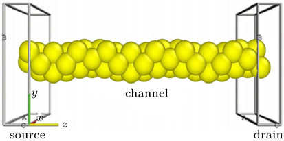 | Fig. 1. (color online) The schematic of the computational models. The supercell particle number of lead nanowire is 20 and the length of electrodes is 63 Å. |
The quantum electron transport properties of lead nanowires are calculated using the NEGF combined with the DFT by the softpackage Atomistix ToolKit,[18,24–26] which can simulate the electrical properties and quantum transport properties of nano structures and nano devices.[26] Double-zeta single polarized basis sets are adopted for the local atomic numerical orbitals, and norm-conserving pseudo-potentials are employed. The exchange correlation function is treated by the Perdew–Burke–Ernzerhof (LEADE)[27] generalized gradient approximition (GGA). The energy mesh cutoff is set to be 150 Ha. The k-point grid mesh is sampled by 1× 1× 100 utilized in the Brillouin zone integration. An electron temperature is 300 K. The energy convergence criterion is set to 10−4 eV. The current I through the device is an integral of the electron transmission probability over the energy, which is obtained from the Landauer–Büttiker equation where the quantity 

Figure
It is expected that such a unique structure would have novel electronic properties. To shed light on the electronic transport properties of these wires, we examined the current–voltage (I–V) characteristic curves to represent the electronic transport probability of lead nanowires. Figure 
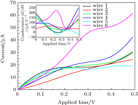 | Fig. 3. (color online) I–V characteristic curves of lead nanowires with different diameter. The inset is the conductance spectra of the six lead nanowires. |
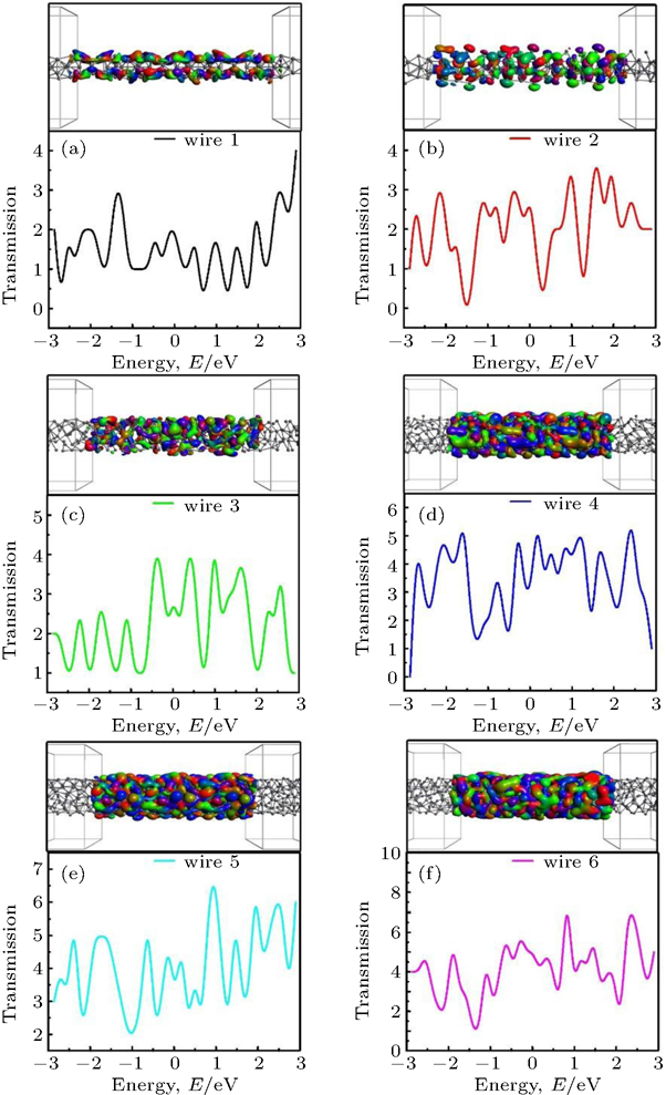 | Fig. 4. (color online) The electronic transmission spectrum of the nanowires at free applied bias (0.0 V). Each inset shows their isosurface plots of the transmission eigenstates at  |
The transmission profiles of these nanowires are shown in Fig. 


We further decomposed the electronic transmission at the Fermi level of these wires as shown in Table 

| Table 1.
The transmission eigenvalues of lead nanowires with different diameter. . |
To further explore more electronic transmission properties, figure
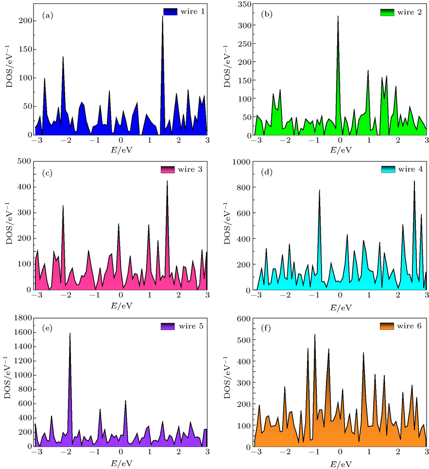 | Fig. 5. (color online) DOSs for (a) wire 1, (b) wire 2, (c) wire 3, (d) wire 4, and (e) wire 5. The zero of energy axis is the Fermi level. |
As for wire 1, there is one prominent peak at −2.16 eV in the valence band region and some weak peaks in the conduction band region, out of which the highest magnitude peak appears at about 1.48 eV. The DOS of wire 2 shows few strong peaks in the valence band region, out of which the highest one appears at −1.6 eV and a strong peak also appears in the conduction band region at 0.76 eV, which defends less localization of states near the Fermi level. While for wire 3, a significant peak appears in the conduction band and a weak peak at 0.1 eV very close to the Fermi level. As for wire 4, there is one prominent peak at −0.7 eV in the valence band region and some weak peaks in the conduction band region, out of which the highest magnitude peak appears at 2.4 eV. For wire 5, the highest peak appears at −2.34 eV near the Fermi level and a prominent peak exists at 1.5 eV in the conduction band region which defends less localization of states near the Fermi level. The DOS for wire 6 shows few strong peaks in the valence band region, out of which the highest one appears at −0.24 eV and a strong peak also appears in the conduction band region at 2.08 eV, which defends less localization of states near the Fermi level.
We further computed projected DOS (PDOS) as shown in Fig. 
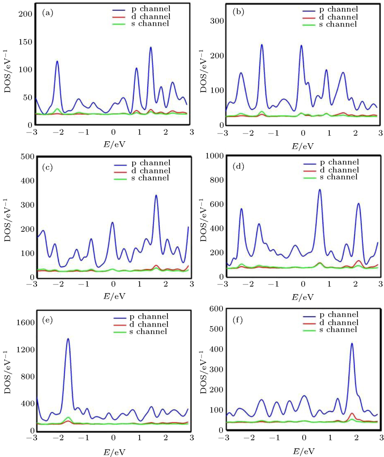 | Fig. 6. (color online) PDOSs for (a) wire 1, (b) wire 2, (c) wire 3, (d) wire 4, and (e) wire 5. The zero of energy axis is the Fermi level. |
Si, Ge, Sn, and Pb are in the same main group in the periodic table of elements. Therefore, their structures and properties may be similar in some extent. We can learn from the previous work that these four kinds of nanowires are all spiral winding and get shifted as the diameter changes. Compared to the result from the research of Zhang,[17] the conductance spectrum (G–V) of the Pb nanowire is quite different from those of Sn, Si, and Ge nanowires. In the same range from 0 to 0.5 V, the Pb device has a more stable conductivity than that of other element devices and does not show a negative differential resistance (NDR) effect. That is because that the conductance spectra of Si, Ge, and Sn nanowires have many irregular peaks, and the transmission spectra of Pb nanowires do not show the gap around Fermi level while the other three do. We conclude that Pb nanowire has more stable electrical properties, indicating that Pb nanowire would be a better candidate for the new generation of nanowire transistors.
We investigate the structures and electronic transport properties of lead nanowires by the GA process and the NEGF method with the DFT frame. Helical structures with different helix degrees are found in lead nanowires. Due to the quantum size effect, the I–V characteristic curves of the nanowires are nonlinear, which do not follow Ohm’s law. The thickest nanowire shows great transmission at the Fermi level because of the strong delocalized electronic state. In addition, the transmission spectrum and DOS show that transmission properties are dependent on the diameter of the nanowires. The nanowire with the maximum diameter has excellent performances, holding promising application in electronic devices. This study provides insight into the relation between the transport property and the diameter of nanowires.
| [1] | |
| [2] | |
| [3] | |
| [4] | |
| [5] | |
| [6] | |
| [7] | |
| [8] | |
| [9] | |
| [10] | |
| [11] | |
| [12] | |
| [13] | |
| [14] | |
| [15] | |
| [16] | |
| [17] | |
| [18] | |
| [19] | |
| [20] | |
| [21] | |
| [22] | |
| [23] | |
| [24] | |
| [25] | |
| [26] | |
| [27] | |
| [28] | |
| [29] | |
| [30] | |
| [31] |


