O3 fast and simple treatment-enhanced p-doped in Spiro-MeOTAD for CH3NH3I vapor-assisted processed CH3NH3PbI3 perovskite solar cells
Jia En-Dong1, 2, Lou Xi1, 3, Zhou Chun-Lan1, 2, †, Hao Wei-Chang3, ‡, Wang Wen-Jing1, 2
The Key Laboratory of Solar Thermal Energy and Photovoltaic System, Institute of Electrical Engineering, Chinese Academy of Sciences, Beijing 100190, China
University of Chinese Academy of Sciences (UCAS), Beijing 100049, China
Department of Physics and Key Laboratory of Micro-nano Measurement, Manipulation and Physics, Beihang University, Beijing 100191, China


† Corresponding author. E-mail: chunlzhou@gmail.com whao@buaa.edu.cn

Project supported by the National Natural Science Foundation of China (Grant Nos. 51472016 and 51272015).

Abstract

We demonstrate a simple and fast post-deposition treatment with high process compatibility on the hole transport material (HTM) Spiro-MeOTAD in vapor-assisted solution processed methylammonium lead triiodide (CH3NH3PbI3)-based solar cells. The prepared Co-doped p-type Spiro-MeOTAD films are treated by O3 at room temperature for 5 min, 10 min, and 20 min, respectively, prior to the deposition of the metal electrodes. Compared with the traditional oxidation of Spiro-MeOTAD films overnight in dry air, our fast O3 treatment of HTM at room temperature only needs just 10 min, and a relative 40.3% increment in the power conversion efficiency is observed with respect to the result of without-treated perovskite solar cells. This improvement of efficiency is mainly attributed to the obvious increase of the fill factor and short-circuit current density, despite a slight decrease in the open-circuit voltage. Ultraviolet photoelectron spectroscopy (UPS) and Hall effect measurement method are employed in our study to determine the changes of properties after O3 treatment in HTM. It is found that after the HTM is exposed to O3, its p-type doping level is enhanced. The enhancement of conductivity and Hall mobility of the film, resulting from the improvement in p-doping level of HTM, leads to better performances of perovskite solar cells. Best power conversion efficiencies (PCEs) of 13.05% and 16.39% are achieved with most properly optimized HTM via CH3NH3I vapor-assisted method and traditional single-step method respectively.

1. Introduction

Organometal halide perovskite solar cells are dramatically emerging as one of the most competitive solar technologies and revolutionizing the field of photovoltaics.[14] With desirable physical properties including broadly tunable bandgaps,[5] high absorption coefficients,[6] high carrier mobilities,[7] extremely long carrier diffusion lengths,[8,9] and good crystallinity,[10,11] organometal halide perovskite materials have been demonstrated to be excellent photovoltaic materials. Since the first version of the perovskite solar cell based on the sensitizer concept in 2009,[12] the power conversion efficiencies (PCEs) of perovskite-based devices have been enhanced from 3.8%[12] to 22% or more.[13] With the continuous development of the perovskite solar cells, this photovoltaic technology will achieve economic feasibility in the near future.

The common device structure of perovskite solar cells consists of a transparent conductive substrate, a compact TiO2 hole-blocking layer, an organolead halide perovskite light-absorption layer combined with a porous scaffold, a hole transporting layer, and a metal counter electrode. Studies have mainly focused on hole-blocking layer optimization,[14] scaffold layers design,[10,15] high quality perovskite film formation methodologies,[16,17] alternative device structure,[18,19] and inherent mechanisms.[9,20,21] Hole transport material (HTM), as one of the key components in perovskite solar cells, separates photo-excited electron–hole pairs and transports the holes to the external circuit.[22] Therefore, the performance of perovskite solar cells is highly dependent on the properties of HTM. The -tetrakis (N,N-di-p-methoxyphenyl-amine)- -spirobifluorene (Spiro-MeOTAD) is the most widely used and the best hole transport material in performance. Because of the high resistivity of the pristine Spiro-MeOTAD, additives like lithium bis (trifluoromethanesulfonyl) imide (Li-TFSI) and 4-tert-butylpyridine (t-BP) are used to dope (p-type) Spiro-MeOTAD to improve its transport property.[23] Among the published reports one adoptable strategy to further enhance its transport property is the oxidation process of Spiro-MeOTAD, such as annealing in dry O2 for more than 10 h at 65 °C[24] and in air over night at room temperature[25] to improve the performance of the device. However, this time consuming process results in less cost-effectiveness.

In the present work, we investigate the CH3NH3PbI3-based device with a structure of glass/fluorine-doped tin oxide (FTO)/TiO2 compact layer/mesoporous TiO2layer/ CH3NH3PbI3/Co-doped p-type Spiro-MeOTAD/silver (Ag). The perovskite films are prepared via vapor-assisted solution processed deposition method.[26] The HTM films are treated in dry O3 at room temperature for 3 different lengths of time: 5 min, 10 min, and 20 min, before evaporating Ag metal contact. The control samples are completely fabricated without O3 treatment. It is observed that the performances of CH3NH3PbI3-based devices are strongly affected by the O3 treatment of the films, which leads to a substantial increase in the PCE of the device with the significant increase of the fill factor and current density. The processing conditions and corresponding results will be discussed in detail.

2. Experiment

CH3NH3PbI3-based perovskite solar cells were fabricated under ambient condition. The x-ray diffraction (XRD), scanning electron microscope (SEM), UV-visible spectroscopy, ultraviolet photoelectron spectroscopy (UPS) and Hall effect measurement are used to characterize the material; I-V measurement is used to determine the photovoltaic performance of device.

2.1. Solar cell fabrication

The 35 mm × 35 mm square substrates, fluorine-doped tin oxide coated glasses (10 Ω/sq), were cleaned by ultrasonication in a detergent diluted washing solution, rinsed with deionized water and ethanol, dried in nitrogen, and then treated under O3/ultraviolet for 30 min.

The clean FTO glasses were coated with 0.15-M and 0.3-M titanium diisopropoxide bis (acetylacetonate) at 3000 rpm for 30 s subsequently. After being heated on a hotplate at 125 °C for 15 min, the coated substrates were annealed in an oven at 550 °C for 30 min in air. The substrates were treated in 0.05-M TiCl4 aqueous solution at 70 °C for 30 min and rinsed with deionized water, followed by being annealed at 550 °C for 20 min in air to form a compact n-type layer of TiO2 (c-TiO2).

Mesoporous TiO2 films were deposited on the substrates by spin coating TiO2 paste at 3000 rpm for 30 s, followed by being heated on a hotplate at 125 °C for 15 min and annealed at 550 °C for 30 min in air subsequently to form a layer of mesoporous TiO2 (mp-TiO2). The FTO/c-TiO2/mp-TiO2 substrates were preserved in nitrogen at 80 °C for 15 h.

The 460-mg/ml precursor of PbI2 solution was prepared by dissolving PbI2 into DMF, then heated to form clean yellow and clear solution. The PbI2 solution in DMF was spin-coated on the FTO/c-TiO2/ mp-TiO2 substrates at 5000 rpm. for 10 s, and dried at 100 °C for 15 min. CH3NH3I powder was spread out around the PbI2 coated substrates with a petri dish covering on the top, and heated at 120 °C for the desired time to form perovskite films. After cooling down, the as-prepared perovskite films were washed with isopropanol, dried and annealed at 80 °C for 30 min.

The perovskite films were coated with the HTM (Co-doped p-type Spiro-MeOTAD) by using the spin-coating method at 2000 rpm for 20 s. The spin-coated Spiro-MeOTAD films were treated with O3, respectively, for 5 min, 10 min, and 20 min as shown in Fig. 1. Soda-lime glass would prevent UV light from irradiating the sample surface but allow O3 to treat it. A sample without O3 treatment was also prepared for comparison. The space for the UVO-treatment is about 0.5 M (length) × 0.5 M (width) × 0.2 M (height). When the UVO treatment was proceeding, the space should avoid circulation of air.
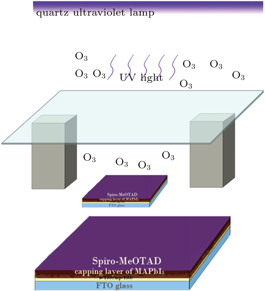
Fig. 1. (color online) Schematic procedure for the fast O3 treatment to Spiro-MeOTAD films. Soda-lime glass excludes the direct UV rays.

Finally, the counter electrode was deposited by thermal evaporation of silver under a vacuum of 5 × 10⁻⁵ Torr (1 Torr = 1.33322 × 10² Pa). The active area was a bit larger than 0.07 cm2 and was finally tested with a mask whose area was just 0.07 cm2.

2.2. Characterization method

The IV characteristics of the devices were measured by using the Keithley 2400 source meter under the calibrated solar simulator equipped with an AM 1.5 filter at 100 mW/cm2. The IV curves were obtained from the reverse scan at a scan rate of from 1.2 V to −0.2 V. The surface morphologies of the films were characterized by scanning electron microscopy (SEM) using the CARL ZEISS-SIGMA field emission scanning electron microscope. UV-visible spectroscopy was performed by using the Varian-Cary 500. X-ray diffraction (XRD) was determined by using the Bruker-D8 Advance in steps of 0.01° for 2θ from 10° to 60°.

Ultraviolet photoelectron spectroscopy (UPS) analysis was conducted by using Beijing synchrotron radiation light source. The charging effects were taken into account by referring the measured spectra to the binding energy peak of Au 4f at 84 eV. The conductivity and Hall mobility were recorded on the HL5500PC Hall Effect measurement system for Co-doped p-type Spiro-MeOTAD film deposited on a 0.5 cm × 0.5 cm2 square glass substrate.

3. Results and discussion

CH3NH3PbI3-based solar cells are fabricated via vapor-assisted solution process.

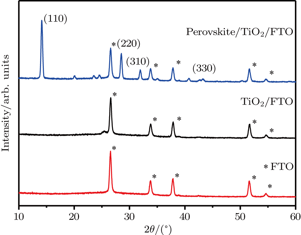
Figure 2 shows the corresponding XRD of the as-prepared CH3NH3PbI3 film on FTO/TiO2 substrate. It provides evidence for the high crystalline nature of our sample and shows the tetragonal perovskite pattern with peaks at 14.13°, 28.52°, 31.93°, 43.22°, corresponding to (110), (220), (310), and (330) respectively, which are in good agreement with previously reported results.[26,27] The broad absorption spectrum of CH3NH3PbI3 is shown in Fig. 3, indicating the strong photon harvesting capability of the material over the spectral range from 400 nm to 800 nm, which is in agreement with the band gap of 1.5 eV for CH3NH3PbI3. The morphologies of the samples have been investigated by scanning electron microscopy (SEM) and the images of typical films are presented in Fig. 3. From the top-view image of CH3NH3PbI3 formed on meso-TiO2 layer, crystalline domains of perovskite with grain size in a range from 200 nm to 400 nm with good surface coverage are observed. As incomplete coverage of perovskite results in undesired shunting paths and minimizes light absorption in solar cells, high surface coverage is important for high performance devices.[24] In addition, crystals with large grain size and good crystalline quality are shown to be favorable for charge transport by suppressing charge trapping during solar cell operation. Thus, they are preferable for the development of high performance devices.[28]
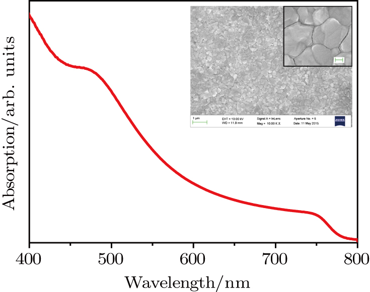
Fig. 2. (color online) XRD patterns of fluorine-doped tin oxide (FTO, red curve), c-TiO2 and meso-TiO2 on FTO (FTO/TiO2, black curve), and metal organic halide perovskite (FTO/TiO2/Perovskite, blue curve).
Fig. 3. (color online) Absorption spectrum of CH3NH3PbI3 film and top-view SEM images for the sample of FTO/TiO2/CH3NH3PbI3. (Insert image with higher resolution, scale bar: 100 nm).

The changes of the electronic properties of the as prepared Spiro-MeOTAD film and film after O3 exposure are probed by UPS with a synchrotron radiation light source. As can be seen in Fig. 4 the leading edge of the highest occupied molecular orbital (HOMO) with respect to the Fermi level for the as-prepared sample is at 0.58 eV. After the first 5-min exposure to O3, the HOMO level of the Spiro-MeOTAD film shows a slight shift toward low binding energy settling at 0.49 eV, illustrated by the green curve. An additional 5-min O3 treatment induces further shift, bringing the HOMO leading edge to −0.44 eV. With a total treatment time of 20 min, the HOMO shows an obvious shift with the leading edges at −0.3 eV, illustrated by the blue curve. This is indicative of improved p-type doping level of Spiro-MeOTAD film with the increase of the time of exposure to O3. Oxygen has been reported to be essential for the doping mechanism of Spiro-MeOTAD. Cappel et al. suggested that the oxygen acts as an electron accepter in an in situ oxidation of Spiro-MeOTAD in solid state dye-sensitized solar cells.[29] Similarly, ozone as a powerful oxidant can efficiently oxidize Spiro-MeOTAD and enhance its doping level.
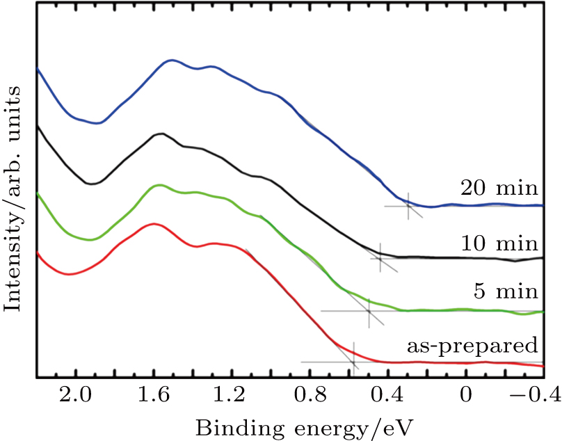
Fig. 4. (color online) UPS corresponding to the HOMO region of the as-prepared sample and samples with different O3 treatment times.

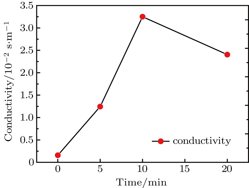
To record the carrier density, Hall mobility and conductivity of the Co-doped p-type Spiro-MeOTAD film, the Hall effect measurement is adopted. The sample is obtained by spinning on 0.5 cm × 0.5 cm square glass at 2000 rpm for 20 s. The thickness of the film is 500 nm. Hall mobility (μ), sheet carrier density ( ), and conductivity (σ) of the as-prepared Spiro-MeOTAD film are measured at room temperature by the van der Pauw method. This sample is re-measured several times after O3 treatment for 5 min, 10 min, and 20 min. Hall mobility and sheet carrier density are shown in Fig. 5. Longer O3 treatment time results in larger carrier density. As O3 treatment enhances the p-type doping level in Spiro-MeOTAD film as shown in Fig. 4 it is easy to understand the increased trend of carrier concentration with the increase of holes as the dominant carriers. Additionally, the hole mobility of Spiro-MeOTAD film increases with the sheet charge density increasing from 6.7 × 108 cm−2 to 1 × 109 cm−2 and reaches the peak at 10-min O3-treatment. This trend is consistent with previously reported results of charge-density-dependent mobility for this material, while the exact values of hole mobility and charge density differ somehow from the values of previously reported results because of the differences in sample structure and measuring method.[30] However, as the hole–hole scattering may suppress the mobility, a decrease in hole mobility can be observed from Fig. 5 with the further increase of the charge density when additional O3 treatment is performed. The conductivity originating from the electron charge is shown in Fig. 6. The variety of conductivity is generally coincident with that of hole mobility, showing a strong dependence on the O3 exposure time. Similar result of reduction in the resistance of the Spiro-MeOTAD layer after annealing in O2 ambient at 65 °C for 12 h has also been reported previously.[24] As a result, the best mobility and conductivity of Spiro-MeOTAD film are obtained with 10 min O3 treatment.
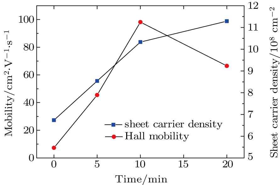
Fig. 5. (color online) Time-dependent carrier mobility and sheet carrier density of the spin-coated Spiro-MeOTAD film on glass substrate.
Fig. 6. (color online) Conductivity of the spin-coated Spiro-MeOTAD film on glass substrate versus O3 treatment time.

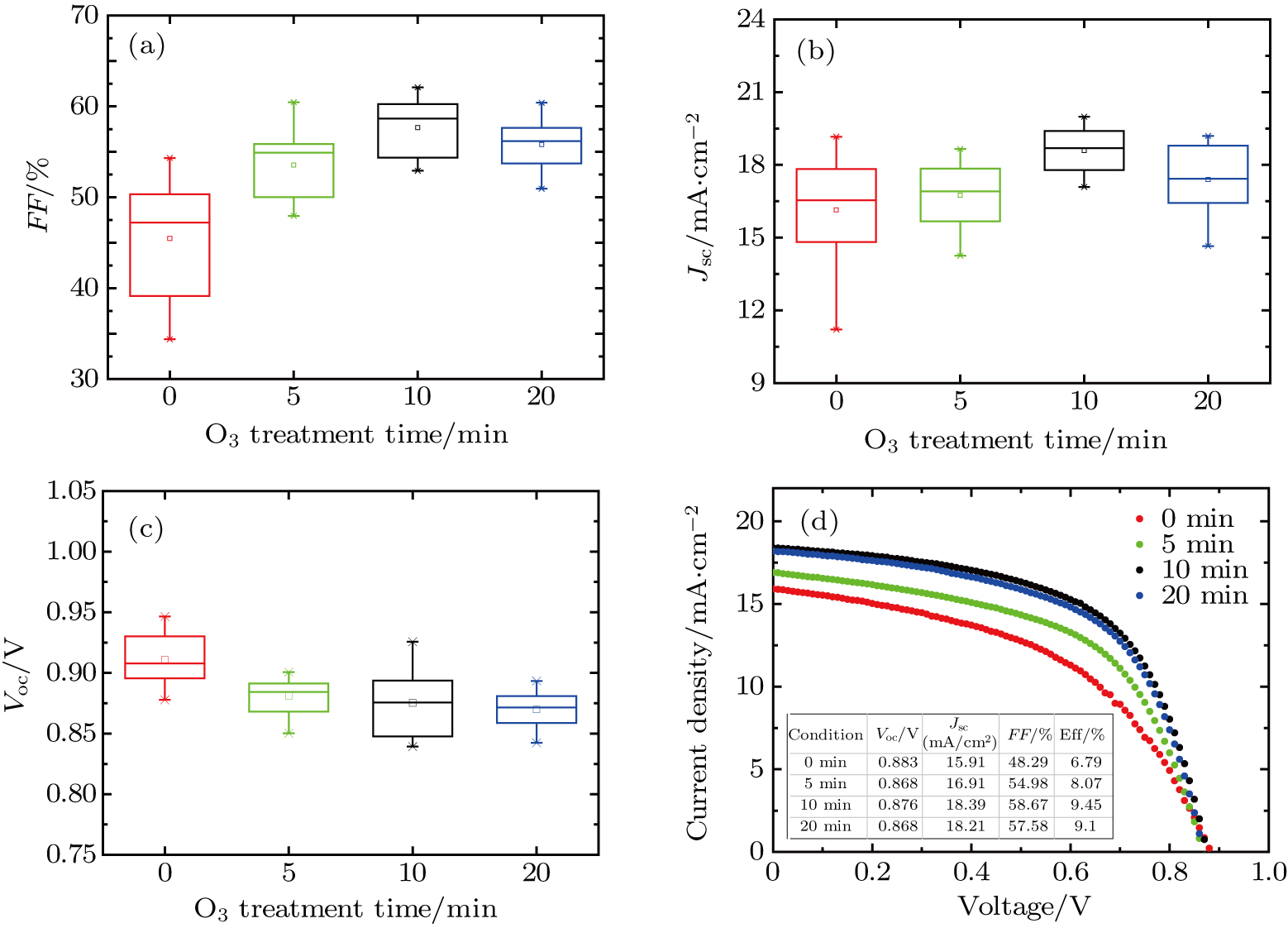
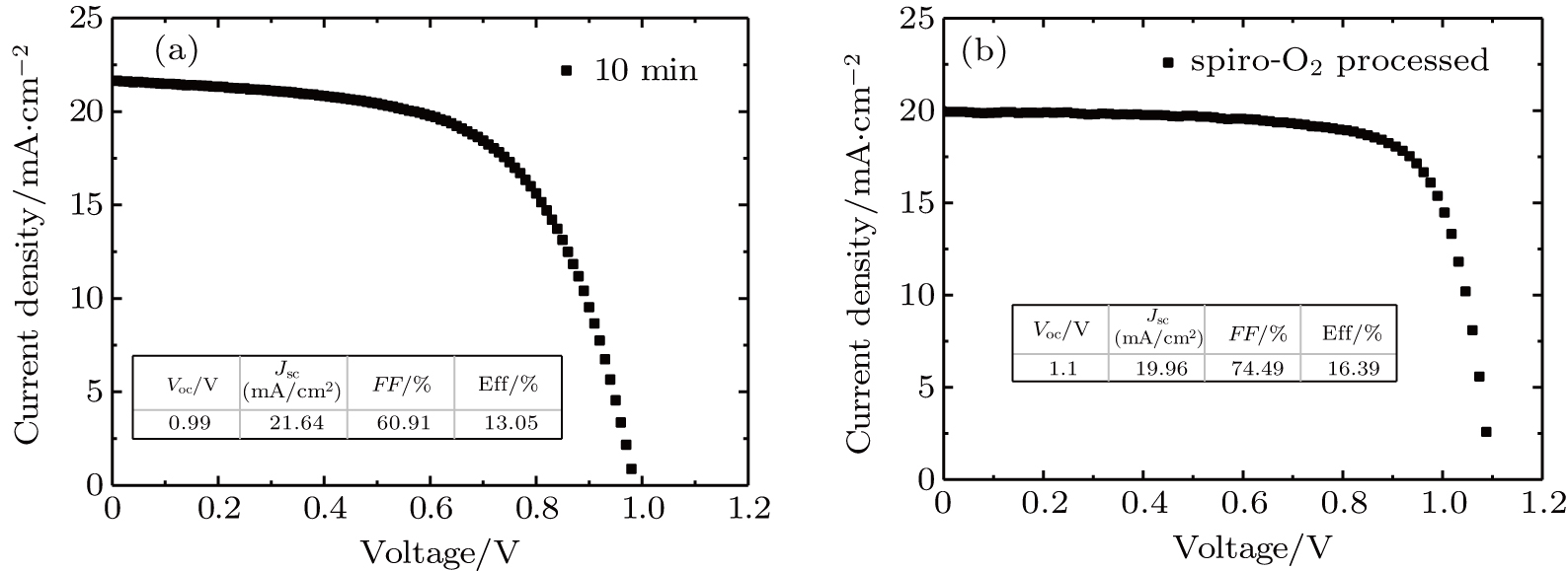
To further confirm the effect of O3 treatment, we examine the exposure-time-dependent photovoltaic performance of CH3NH3PbI3-based solar cells employing Spiro-MeOTAD as HTM with different exposure times. JV curves of average performance devices as representative devices are shown in Fig. 7(d). The relationships of serial resistance ( ), fill factor (FF), short-circuit photocurrent density , open-circuit voltage , and efficiency (η) with O3 treatment are presented in Figs. 6 and 7(a)7(d). In comparison with the control group, devices with O3 treatment yields better performance with the increase of and FF, despite a slight decrease in . As shown in Fig. 6, the average series resistance ( ) of device without O3 treatment is 20.2 Ω. It substantially decreases to 11.8 Ω after 5-min O3 treatment. With an additional 5 min treatment, drops to the bottom of 8.1 Ω. Then, it increases slightly to 9.0 Ω with a total of 20-min treatment. It is well known that the represents the total resistance of the cell and is a resultant resistance of the active and interfacial layer resistances, electrode resistances, and the various contact and interconnect resistances.[31] Combining with results from Hall effect measurement, it is reasonable to believe that the conductivity and mobility increase of hole transport layer increase the series resistance. can have a pronounced effect on the solar cell fill factor (FF), and FF is often the dominant parameter determining the power conversion efficiency. The lower enables a large FF.[14] In Fig. 7(a), average FF substantially increases from 45.48% without O3 treatment to 53.54% with 5-min treatment, corresponding to the opposite trend of . An additional 5-min treatment induces an increase, obtaining FF of 57.67%, while the further increase of the O3 treatment time to 20 min results in a reduction in FF. According to Fig. 7(b), short-circuit photocurrent density ( ) shares the same trend with FF. Devices with O3 treatment yields higher than devices without O3 treatment. The improved suggests that the carrier collection efficiency across the perovskite/ Spiro-MeOTAD interface is improved. This may result from the hole mobility enhancement, thus improving the hole transport in HTM. In addition, 10-min exposure achieves optimization with of 18.59 mA/cm2 on average, while less or further exposure induced a decline in , consistent with the result of hole mobility. The open circuit voltage ( ) decreases slightly with O3 treatment increasing, but the reason is not clear. As a result, the average conversion efficiency of Spiro–MeOTAD film increases from 6.7% without O3 treatment to 9.4% with 10-min oxidation process, corresponding to 40.3% increment. The best performance device achieves η of 13.05%, with , , as shown in Fig. 8(a). It is a remarkable fact that the value of η reaches 13% via CH3NH3I vapor-assisted method in ambient air. We also fabricate perovskite solar cells in a strictly controlled ( for both O3 and H2O) glove box via traditional single step.[3237] The best performance of device achieves the η value of 16.39%, with , , as shown in Fig. 8(b). In strictly controlled atmosphere the quality of perovskite film can be much better than in ambient air. We do not discuss more details of this point because the oxidation and doping level of spiro-MeOTAD under O3 are the key points of this article.

Fig. 7. (color online) The average values of photovoltaic parameters obtained from IV measurements for CH3NH3PbI3-based solar cells with different O3 treatment times. (a) FF, (b) , (c) , and (d) JV curves of average performance devices with different O3 treatment times.
Fig. 8. JV curve of the best performance device with the optimized O3 treatment time via (a) vapor-assisted in air and (b) single-step in glove box.
4. Conclusions

In this work, O3 is adopted to treat co-doped p-type Spiro-MeOTAD film at room temperature before evaporating Ag metal contact when fabricating CH3NH3PbI3-based perovskite solar cells under ambient condition. The O3 treatment procedure enhances p-doping level in this hole transport material which is evidenced by the HOMO level approaching Fermi level after O3 treatment. This leads to the increase in the carrier density, improvement in the carrier mobility and optimization in conductivity of Spiro-MeOTAD, which is confirmed by Hall effect measurement. Results suggest that the enhancements in the conductivity and carrier mobility lead to better device performance and 10-min treatment turned out to be favorable for the optimization, thus achieving a 40.3% increment in the PCEs: an averaged enhancement is 9.4%. The values of η reach, respectively, 13.05% in ambient air via CH3NH3I vapor-assisted method and 16.39% in glove box via traditional single-step method, indicating that the device achieves the best performance. This presents a short-time and effective process to improve the efficiency of organometal halide perovskite solar cells

Reference
[1] Snaith H J 2013 J. Phys. Chem. Lett. 4 3623
[2] Green M A Ho-Baillie A Snaith H J 2014 Nat. Photon. 8 506
[3] Kim H S Im S H Park N G 2014 J. Phys. Chem. C 118 5615
[4] Boix P P Nonomura K Mathews N Mhaisalkar S G 2014 Mater. Today 17 16
[5] Eperon G E Stranks S D Menelaou C Johnston M B Herz L M Snaith H J 2014 Energy Environ. Sci. 7 982
[6] Im J H Lee C R Lee J W Park S W Park N G 2011 Nanoscale 3 4088
[7] Mitzi D B 1999 Progress in Inorganic Chemistry 48 Karlin K D New York John Wiley & Sons Inc. 1 121
[8] Stranks S D Eperon G E Grancini G Menelaou C Alcocer M J P Leijtens T Hertz L M Petrozza A Snaith H J 2013 Science 342 341
[9] Xing G C Mathews N Sun S Y Lim S S Lam Y M Gratzel M Mhaisalkar S Sum T C 2013 Science 342 344
[10] Lee M M Teuscher J Miyasaka T Murakami T N Snaith H J 2012 Science 338 643
[11] Stoumpos C C Malliakas C D Kanatzidis M G 2013 Inorg. Chem. 52 9019 9038
[12] Kojima A Teshima K Shirai Y Miyasaka T 2009 J. Am. Chem. Soc. 131 6050
[13] Yang W S Noh J H Jeon N J Kim Y C Ryu S Seo J Seok S 2015 Science 348 1234
[14] Wu Y Yang X Chen H Zhang K Qin C Liu J Peng W Q Islam A Bi E B Ye F 2014 Appl. Phys. Express 7 052301
[15] Ball J M Lee M M Hey A Snaith H J 2013 Energy Environ. Sci. 6 1739
[16] Im J H Jang I H Pellet N Gratzel M Park N G 2014 Nat. Nanotechnol. 9 927
[17] Nie W Tsai H Asadpour R Blancon J C Neukirch A J Gupta G 2015 Science 347 522
[18] Abu Laban W Etgar L 2013 Energy Environ. Sci. 6 3249
[19] Liu D Yang J Kelly T L 2014 J. Am. Chem. Soc. 136 17116
[20] Gonzalez-Pedro V Juarez-Perez E J Arsyad W S Barea E M Fabregat-Santiago F Mora-Sero I 2014 Nano. Lett. 14 888
[21] Sum T C Mathews N 2014 Energy Environ. Sci. 7 2518
[22] Zhang H Shi Y T Yan F Wang L Wang K Xing Y J Donga Q S Ma T L 2014 Chem. Commun. 50 5020
[23] Schölin R Karlsson M H Eriksson S K Siegbahn H Johansson E M J Rensmo H 2012 J. Phys. Chem. 116 26300
[24] Ren Z W Ng A Shen Q Gokkaya H C Wang J Yang L J Yiu W K Bai G X Djurisic A B Leung W W F 2014 Sci. Rep. 4 6752
[25] Chen H W Sakai N Ikegami M Miyasaka T 2015 J. Phys. Chem. Lett. 6 164
[26] Chen Q Zhou H Hong Z Luo S Duan H S Wang H H Liu Y S Li G Yang Y 2014 J. Am. Chem. Soc. 136 622
[27] Baikie T Fang Y Kadro J M Schreyer M Wei F Mhaisalkar S G Graetzel M White T J 2013 J. Mater. Chem. 1 5628
[28] Nie W Y Tsai H H Asadpour R Blancon J C Neukirch A J Gupta G Crochet J J Chhowalla M Tretiak S Alam M A 2015 Science 347 522
[29] Cappel U B Daeneke T Bach U 2012 Nano. Lett. 12 4925
[30] Leijtens T Lim J Teuscher J Park T Snaith H J 2013 Adv. Mater. 25 3227
[31] Servaites J D Yeganeh S Marks T J Ratner M A 2010 Adv. Funct. Mater. 20 97
[32] Wang T Y Cheng J W Wu G X Li M C 2016 Sci. China-Mater. 59 703
[33] Song D D Cui P Wang T Y Wei D Li M C Cao F H Yue X P Fu P F Li Y Y He Y 2015 J. Phys. Chem. 119 22812
[34] Song D D Wei D Cui P Li M Duan Z Q Wang T Y Ji J Li Y Y Jbengue J M Li Y F He Y Trevor M Park N G 2016 J. Mater. Chem. 4 6091
[35] Zhang Z R Yue X P Wei D Li M C Fu P F Xie B X Song D D Li Y F 2015 RSC Adv. 5 104606
[36] Wei D Ji J Song D D Li M C Cui P Li Y Y Mbengue J M Zhou W J Ning Z J Park N G 2017 J. Mater. Chem. 5 1406
[37] Cui P Fu P F Wei D Li M C Song D D Yue X P Li Y Y Zhang Z R Li Y F Mbengue J M 2015 RSC Adv. 5 75622