Low temperature ferromagnetic properties of CdS and CdTe thin films
Masood Hafiz Tariq1, Muhammad Zahir2, Habib Muhammad2, Wang Dong-Ming1, Wang De-Liang1, ‡
Hefei National Laboratory for Physical Science at the Microscale, University of Science and Technology of China, Hefei 230026, China
National Synchrotron Radiation Laboratory, Center for Excellence in Nanoscience, Chinese Academy of Sciences, University of Science and Technology of China, Hefei 230026, China


† Corresponding author. E-mail: eedewang@ustc.edu.cn

Abstract

The magnetic property in a material is induced by the unpaired electrons. This can occur due to defect states which can enhance the magnetic moment and the spin polarization. In this report, CdS and CdTe thin films are grown on FTO glass substrates by chemical bath deposition and close-spaced sublimation, respectively. The magnetic properties, which are introduced from oxygen states, are found in CdS and CdTe thin films. From the hysteresis loop of magnetic moment it is revealed that CdS and CdTe thin films have different kinds of magnetic moments at different temperatures. The MH curves indicate that from 100 K to 350 K, CdS and CdTe thin films show paramagnetism and diamagnetism, respectively. A superparamagnetic or a weakly ferromagnetic response is found at 5 K. It is also observed from ZFC/FC curves that magnetic moments decrease with temperature increasing. Spin polarized density functional calculation for spin magnetic moment is also carried out.

1. Introduction

Magnetic materials are important materials due to their many applications in different fields including medical application, energy generation, microwave communication, and data storage.[17] It is important to study the origins of magnetism in materials in order to fabricate devices based on magnetic materials.[8] Researchers are beginning to investigate a variety of materials which have been studied relatively little before and exploring their unperceived magnetic behaviors.

A few of these materials are cadmium sulfide CdS and cadmium telluride CdTe, which are both II–IV group semiconductors. Although tremendous work has been done on the studies of optical properties of these materials, so far the work on their magnetic properties is still limited. The CdS and CdTe are suitable candidates for the use as host materials in different applications.[9,10] Some techniques such as electrode deposition, laser ablation, spray pyrolysis, radio frequency magnetron sputtering, close space vapor transport, and chemical bath deposition (CBD) can be employed to fabricate CdS and CdTe thin films.[1116] The most simple and economical method of growing the CdS thin film is chemical bath deposition which can yield uniform and nearly stoichiometric CdS film at room temperature. CdS has some interesting properties. Its direct band gap value is 2.42 eV that makes it a suitable candidate for a number of applications which are beneficial for enhancement of device performance. The CdS film is used as a window layer in solar cell fabrication, photodetectors, piezoelectric transducers, and bolometers.[9,10,17] CdTe has a band gap of 1.45 eV, a high electron affinity of 4.5 eV and a high work function of 5.7 eV.[18] CdTe has been used in some areas, such as CdTe thin film used as an absorber layer of solar cell, integrated optics, optoelectronics, gamma ray detection, and x-ray imaging.[19,20] CdTe can be fabricated by different techniques including electro-deposition, molecular beam epitaxial, metal–organic chemical vapor deposition, screen printing, and close-spaced sublimation.[21] In this work, we fabricate CdTe thin films by a home-made close-spaced sublimation method (CSS). There are many fundamental problems related to the materials, which are needed to be studied in a consistent way. One of them is about the physical properties of these materials under different external environments. In this study, the magnetic responses in CdS and CdTe thin films under low and high temperatures are investigated, the MH curves are measured, and some interesting properties in CdS and CdTe thin films are found.

2. Experiments

Close-spaced sublimation method was used to fabricate the CdTe thin films. CdTe films were grown on glass substrates coated with transparent conducting oxide (FTO). The source and substrate temperatures were 670 °C and 540 °C, respectively. The spacing between source and substrate was 3 mm, the deposition atmosphere was a mixture of O and Ar. The total pressure of Ar and O was 2000 Pa in which the oxygen partial pressure was 200 Pa. The thickness of CdTe films was μm. The CdTe films were heat treated in the presence of CdCl in the air atmosphere at 400 °C. The CdS films were fabricated on glass substrates with a thickness of nm by chemical bath deposition technique (CBD). The solution was prepared at room temperature by mixing deionized water, ammonium hydroxide, cadmium acetate, and thiourea. The solution was kept at 85 °C during the deposition of CdS. After CdS deposition the samples were rinsed with DI water and then dried with nitrogen gas. The CdS films were then spin-coated with a saturated CdCl methanol solution before transferred into a tube furnace which had been pre-heated to a temperature of 410 °C. The heat treatment was carried out in a CdCl and air atmosphere. The CdS films were then etched in hydrazine hydrate for 15 min to remove oxide formed during the CdCl heat treatment. Finally the CdS films were rinsed with DI water at a temperature of around 80 °C. The fabricated CdS thin films each had a crystalline structure with a mono-grain layer.[22]

The film morphological microstructures were characterized by using a field emission scanning electron microscope (SEM, Sirion 200). XPS measurements were performed by using a Thermo VG Scientific ESCALAB 250 instrument with Al Kα as the x-ray source. All the XPS spectra were calibrated by using the carbon 1s peak (284.6 eV). High resolution x-ray diffraction (XRD) was carried out to characterize the film structure. The magnetic moments of the CdS and the CdTe thin films were measured by using a vibrating sample magnetometer (VSM). Superconducting quantum interference device (SQUID, quantum design MPMS XL-7) magnetometer was employed for VSM. The magnetic moment was measured by using VSM in a temperature range of 5 K–350 K.

3. Results and discussion

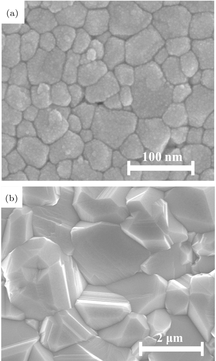
Figure 1(a) shows the surface morphology of a CdS film that is deposited on an FTO coated glass substrate. The CdS film is heat treated in air with CdCl vapor. It consists of a mono-grained layer of CdS grains. The sizes of CdS grains are between 80 nm–100 nm and the grains are densely packed on the FTO/glass substrate. Figure 1(b) shows the microstructured surface image of a CdTe thin film, which has been heat-treated in the presence of CdCl . The CdTe grain size is μm–2 μm, which is the optimum grain size for fabricating the high-efficient CdTe solar cell.[22]

Fig. 1. SEM microstructure images of (a) a mono-grained CdS and (b) CdTe thin film.

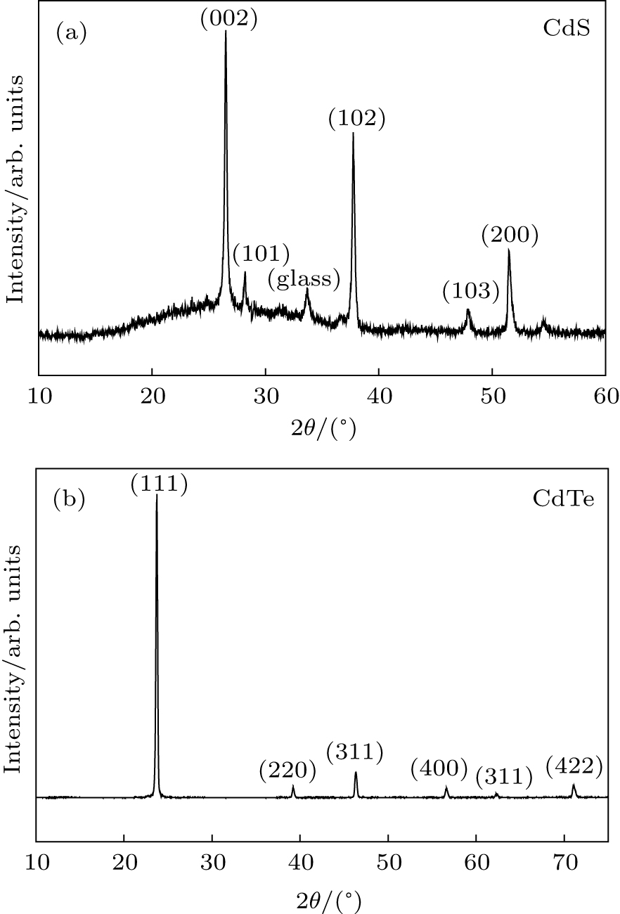
Figure 2 shows the XRD spectra of a CdS and a CdTe thin film. In the CdS thin film, there appears a strong diffraction peak at corresponding to the H (002) hexagonal and the C (101) cubic phase. Other peaks are corresponding to hexagonal (102) and (200) phases. We also perform heat treatment with a CdCl -coating at 410 °C for the CdS film, and the intensities of diffraction peaks are increased. The peaks are correlated to the CdS hexagonal phase, and the full widths at the half maximum (FWHMs) of the (102) and (200) peaks are relatively narrow. The grain size of the CdCl -annealed film is estimated to be about 89 nm by using the Scherer formula. This result is in good agreement with that of SEM. Figure 2(b) shows the XRD pattern of the CdTe film. A strong (111) texture orientation together with low-intensity peaks of (220), (311), (400), (331), and (422) is observed. In a densely packed CdTe film, which has grains with sizes on the order of micrometer, the XRD result is consistent with the reported result for CdTe film prepared by physical vapor deposition which usually produces CdTe film with relatively large grain size. Such a CdTe film usually does not show much grain growth after the CdCl heat treatment.[23]

Fig. 2. The x-ray spectra of (a) a CdS and (b) a CdTe thin film.

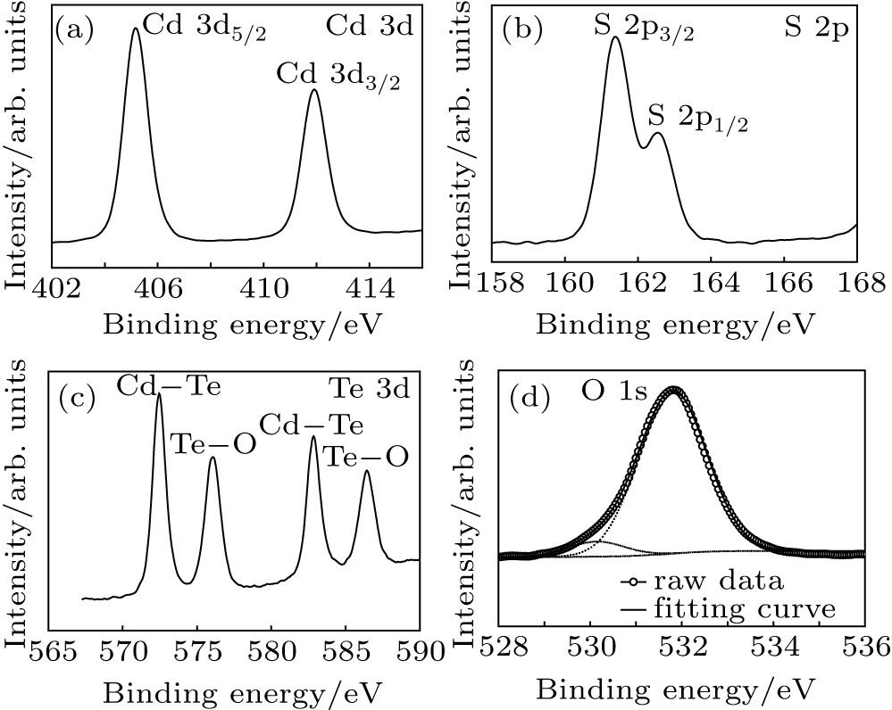
Figure 3 shows the XPS spectra for a CdS and a CdTe film. The two Cd 3d peaks in Fig. 3(a) are from the spin–orbit splitting of the Cd 3d and the Cd 3d states. Figure 3(b) shows that the binding energies of the S 2p and the S 2p peaks for the as-deposited film are 161.2 eV and 162.4 eV, which agrees well with the reported spin–orbit energy splitting of 1.2 eV.[24] The XPS intensity for S reaches a maximum after annealing with CdCl . The Te 3d core-level binding energy is shown in Fig. 3(c). The peaks at 576.10 eV and 586.45 eV are the binding energies of Te 3d and Te 3d in Te–O bond. The two Te–O peaks are observed. These two peaks are detectable from the exposed CdTe surface. The oxygen in the Te–O bond comes from the CdTe preparation process, in which oxygen and Ar are added into the growth chamber during the sublimation. As the film with a CdCl -coating is annealed at 400 °C, the two weak peaks at 572.45 eV and 582.85 eV, which correspond to the binding energies of Te 3d and Te 3d in the Cd–Te bond, are detected, indicating that the surface of the CdTe is composed of CdTeO and CdTe. Due to 400-°C heat treatment, the intensities of the two peaks corresponding to the Te–O bond increasesignificantly. Figure 3(d) shows the binding energy of the O 1s peak. The peak at 531.7 eV is related to the chemically adsorbed surface O atoms on CdTe. The shoulder peak at 530.0 eV is attributed to the Cd–O bond, which is the oxidation product of CdTe with oxygen at the temperature above about 400 °C.[2527] The same trend is observed for CdS thin films and reported in our previous work.[24] We believe that the existence of oxygen peaks in both samples proves that there are some defects in the CdS and the CdTe film due to oxygen vacancy.

Fig. 3. Core-level XPS spectra of (a) Cd 3d of CdTe, (b) S 2p of CdS, (c) Te 3d of CdTe, and (d) the O 1s peaks of CdTe.

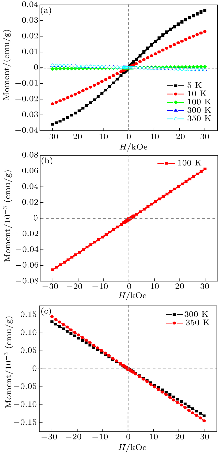
We measure the magnetic moments of the samples by using a vibrating sample magnetometer (VSM) technique at different temperatures to study the magnetic responses of the samples. From the magnetic hysteretic loop we observe the magnetic responses of the growth samples. Figure 4 illustrates the magnetization curves of a CdS thin film at different temperatures. The results reveal that the CdS film has a strong diamagnetic behavior at room temperature (300 K) and also at 350 K. This effect is due to the electron moment in the atoms, and each atom can be regarded as independent response to the applied magnetic field. When an atom in a material has a closed shell structure, the atom as a whole has no net moment. Therefore, CdS thin film has no magnetic moment at room temperature nor at high temperature and behaves as diamagnetism. With temperature decreasing, the net magnetic moment of atoms or ions would increase and exhibits paramagnetism because of the non-cancellation between the spin and orbital components. Therefore the magnetic moment curves suddenly change from diamagnetism to paramagnetism.
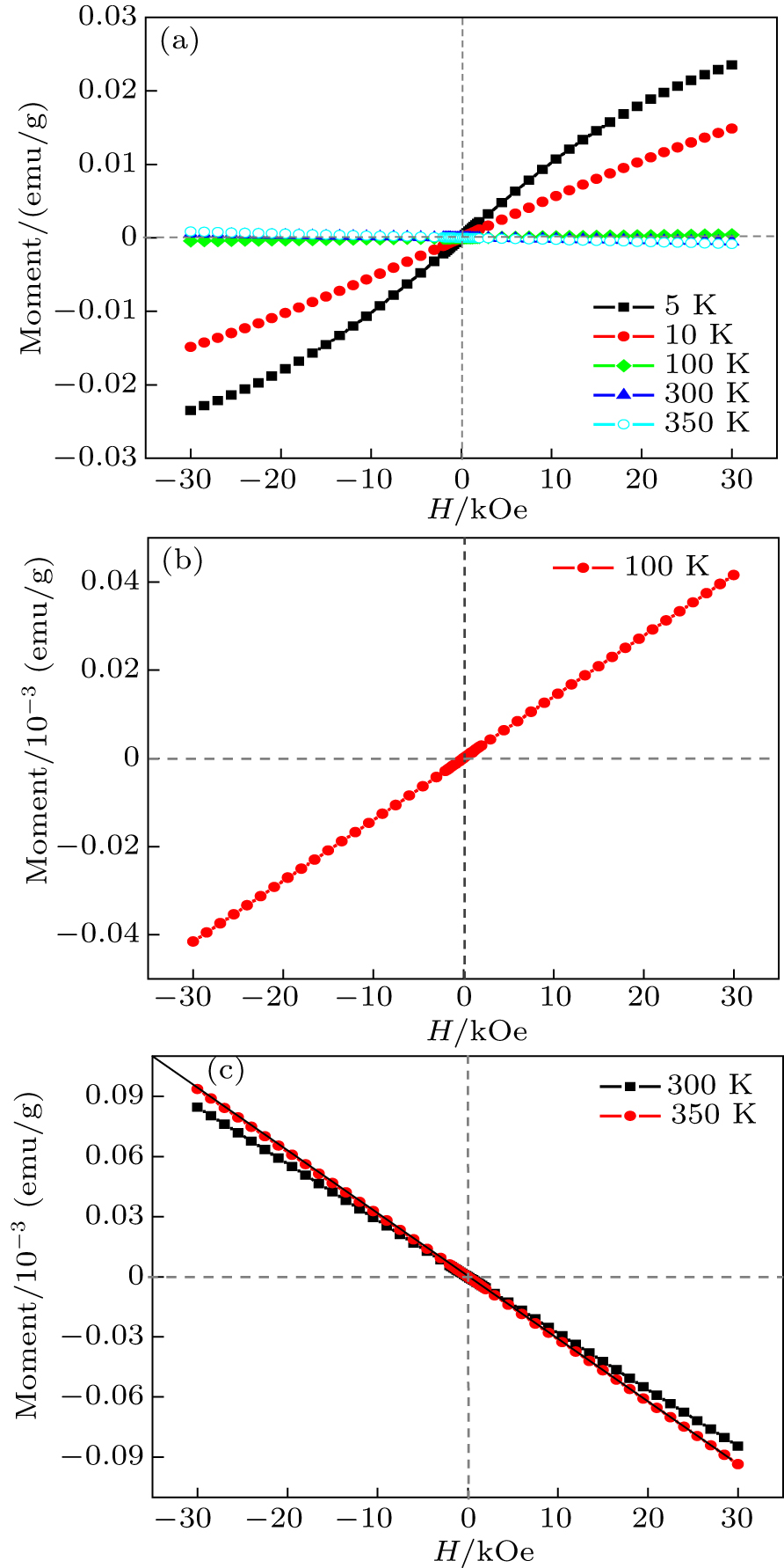
Fig. 4. (color online) MH curves of a CdS thin film measured at (a) 5, 10, 100, 300, and 350 K, (b) 100 K, and (c) 300 K and 350 K, respectively. The unit A .

The paramagnetic response is very high at 10 K compared with that measured at 100 K (Figs. 4(a) and 4(b)). Moreover, by further reducing the temperature, the curve shown in the figure behaves like a hysteresis loop at 5 K, which illustrates that the sample changes from paramagnetism to superparamagnetism or weak ferromagnetism.[28] Hence, at low temperature the CdS thin films behave as ferromagnetism. The saturation magnetic moment per CdS thin film is roughly estimated to be 0.026 at 5 K. Similarly, the MH curves of a CdTe thin film measured at different temperatures are plotted in Fig. 5. The MH curves are measured at 10, 100, 300, and 350 K, respectively. Notably, the MH curves of the CdTe film exhibits the diamagnetism at room and higher temperatures of 300 K and 350 K (see Fig. 5(c)). However, at low temperatures they behave as paramagnetism which can reach to a high value of 0.03 emu/g at 10 K (Fig. 5(a)) compared with at 100 K (Fig. 5(b)). Moreover, at 5 K the hysteresis loop shows that it changes to superparamagnetism or weak ferromagnetism. The maximum magnetization saturation value of the CdTe thin film reaches to a value of 0.04 at a temperature of 5 K. This result is quite fascinating compared with the result reported previously.[29]

Fig. 5. (color online) (a) MH curves of a CdTe thin film measured at (a) 5, 10, 100, 300, and 350 K, (b)100 K, and (c)300 K, and 350 K, respectively.

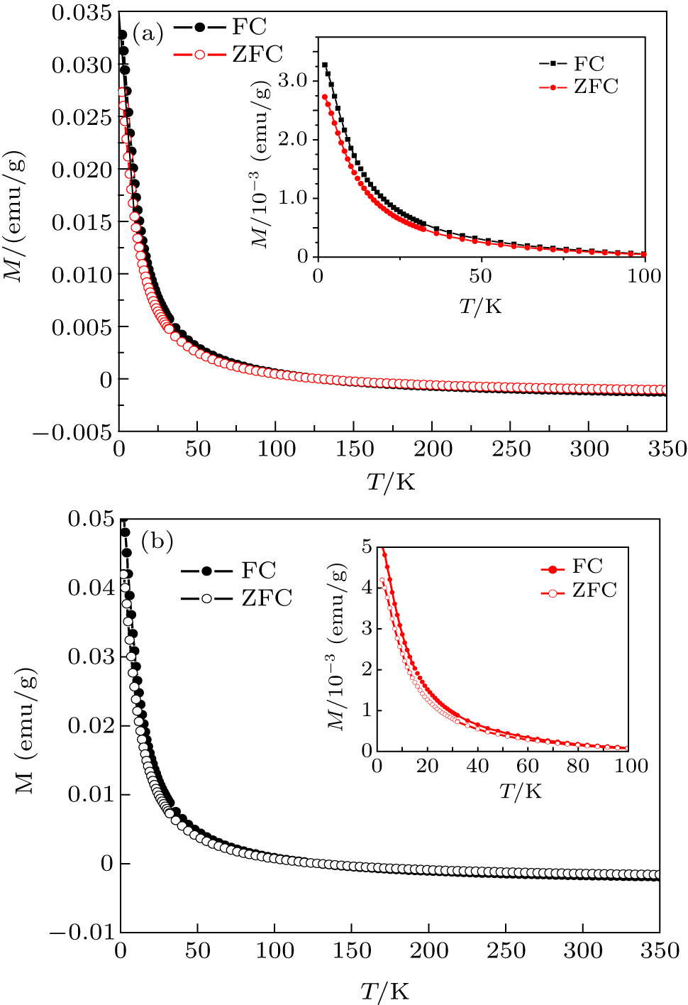
Figure 6 shows the zero-field cooled (ZFC) and field cooled (FC) magnetization curve measured at 400 Oe. Both the FC and the ZFC curves have almost the same behavior in the measured temperature ranges for the CdS and the CdTe thin films. The magnetization value decreases quickly down to 90 K (seen in the insets in Figs. 6(a) and 6(b)) and after that it remains almost unchanged till a temperature of 350 K. The responses of the FC and the ZFC curves shows that the majority of the carriers are localized at the surface of thin films. Different FC and ZFC curves can also show the superparamagnetic or weak ferromagnetic behavior.

Fig. 6. (color online) Zero-field-cooled (ZFC) and field-cooled (FC) magnetization curves of (a) CdS and (b) CdTe thin films measured at 400 Oe.

In addition, many reports have indicated that the magnetic moment is induced by the unpaired electrons and polarization. But the surrounding vacancies, defects and interaction of vacancy–vacancy in the ground state could also enhance the magnetic moments and the spin polarization. Therefore, it suggests that the oxygen defects shown in our XPS results could be the source of magnetism. Ground-state electronic and magnetic properties are studied by the first-principle density functional theory (DFT) calculations with using the spin-polarized plane-wave, which is implemented by Vienna ab-initio simulation package (VASP).[30,31] The generalized gradient approximation (GGA) in Perdew–Burke–Ernzerhof (PBE) is used for the exchange correlation functional and projector augmented wave (PAW) potentials.[32]

The lattice parameters of CdS and CdTe unit cells are taken from our experimental data, respectively. The cut-off energy is set to be 500 eV and the integral number of regular k-points with spaced sampling of is used for optimization. The cut-off energy and k-points for static electronic calculations are set to be 400 eV and , respectively. The spacing between two adjacent layers is larger than 15 Å.

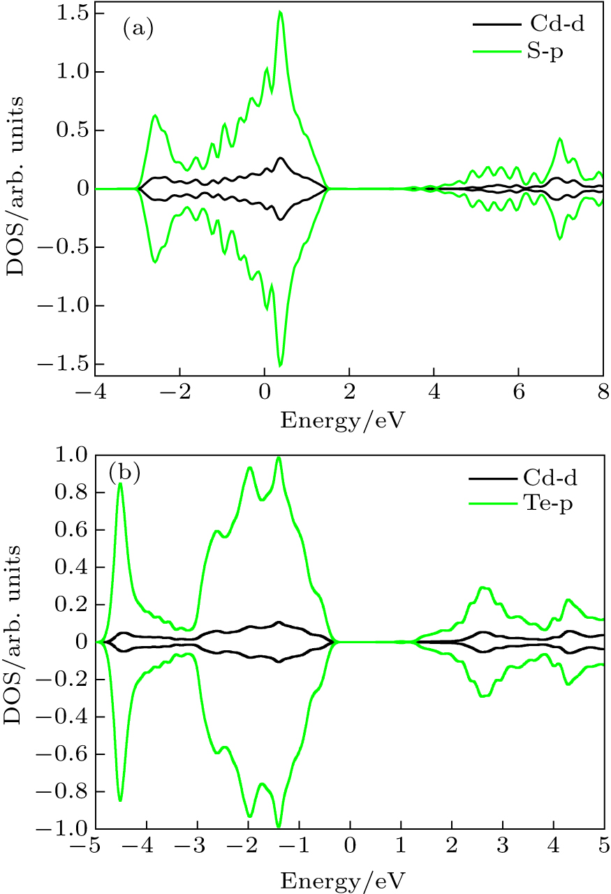
The calculated densities of states for the S-p, the Te-p, and the Cd-d orbitals of CdS and CdTe are shown in Fig. 7. In both CdS and CdTe the electronic structures of electron–electron interaction model are presented. The corresponding densities of states (DOSs) show that when Coulomb correlation is included, both CdS and CdTe around the Fermi-level have strong influence of spin polarization states. And the orbital content of the conduction and valence band edges are most relevant to the study of the carrier-density-dependent magnetic properties as shown from the project partial density of states (PDOS). These results show that the magnetic configuration of the material is due to the valence and conduction band edge of orbital which can be dominated by cadmium (Cd) atoms.

Fig. 7. (color online) PDOS calculations of (a) CdS and (b) CdTe.
4. Conclusions

In summary, CdS and CdTe thin films are fabricated, which behave as superparamagnetism or weak ferromagnetism at low temperature. It is observed from the experimental characterization that the oxygen vacancies could enhance the spin moments between valance and conduction band. The CdS and CdTe thin films at different temperatures show different electronic moments which could change the magnetism of the films. At low temperature the CdS and CdTe thin films exhibit ferromagnetism due to spin moments of electrons in the atoms. The XPS peaks of oxygen imply that the vacancies in the samples could enhance the ferromagnetism. Moreover, from the spin-polarized calculation we observe the spin states of electrons in different orbital states.

Reference
[1] Ramanujan R V 2009 Biomedical Materials New York Springer US 978-0-387-84872-3
[2] Clavijo-Jordan V Kodibagkar V D Beeman S C Hann B D Bennett K M 2012 Nanomed. Nanobiotechnol. 4 345
[3] Laura H Lewis Felix Jimenez-Villacorta 2013 Metall. Mater. Trans. 44 S2
[4] Gutfleisch O Willard M A EkkesBrück Chen C H Sankar S G Liu J P 2011 Adv. Mater. 23 821
[5] Toneguzzo P Viau G Acher O Fiévet-Vincent F Fievet F 1998 Adv. Mater. 10 1032
[6] Horvath M P 2000 J. Magn. Magn. Mater. 215 171
[7] Cowburn R P 2002 J. Magn. Magn. Mater. 245 505
[8] Liu X H Tang Z H Kong Y H Fu X 2016 J. Comput. Electron. 16 115
[9] Bosio A Romeo N Mazzamuto S Canevari V 2006 Prog. Cryst. Growth Ch. 52 247
[10] Lahewil A S Z Al-Douri Y Hashim U Ahmed N M 2012 Sol. Energy 86 3234
[11] Das S 1993 Sol. Energy Mater. Sol. Cells 29 277
[12] Dushkina N Ullrich B Sakai H Segawa Y Hibino K Eiju T 2000 Thin Solid Films 360 222
[13] Ma Y Y Bube R H 1977 J. Elect. Soc. 124 1430
[14] Cong H N Sene C Chartier P 1993 Sol. Energy Mater. Sol. Cells 30 127
[15] Schaffner J Feldmeier E Swirschuk A Schimper H J Klein A Jaegermann W 2011 Thin Solid Films 519 7556
[16] Mahmoud S Ibrahim A Riad A 2000 Thin Solid Films 372 144
[17] Wan L Bai Z Hou Z Wang D Sun H Xiong L 2010 Thin Solid Films 518 6858
[18] Shen K Yang R Wang D Jeng M Chaudhary S Ho K 2016 Sol. Energy Mater. Sol. Cells 144 500
[19] Bai Z Yang J Wang D 2011 Appl. Phys. Lett. 99 143502
[20] Locker M Fischer P Krimmel S Kruger H Lindner M Nakazawa K 2004 IEEE Trans. Nucl. Sci. 51 1717
[21] Shen K Bai Z Deng Y Yang R Wang D Li Q 2016 RSC Adv. 6 52326
[22] Yang R Wang D Wan L Wang D 2014 RSC Adv. 4 22162
[23] Bai Z Wang D 2012 Phys. Status Solidi 209 1982
[24] Wang D Hou Z Bai Z 2011 J. Mater. Res. 26 697
[25] Khallaf H Chai G Lupan O Chow L Park S Schulte A 2009 Appl. Surf. Sci. 255 4129
[26] Bartolo-Pérez P Castro-Rodrıguez R Caballero-Briones F Cauich W Peña J Farias M 2002 Surf. Coat. Technol. 155 16
[27] Niles D W Herdt G Al-Jassim M 1997 J. Appl. Phys. 81 1978
[28] Wang K Y Sawicki M Edmonds K W Campion R P Rushforth A W Freeman A A Foxon C T Gallagher B L Dietl T 2006 Appl. Phys. Lett. 88 022510
[29] Carcia P F Meinhaldt A D Suna A 1985 Appl. Phys. Lett. 47 178
[30] Kohn W Sham L J 1965 Phys. Rev. 140 A1133
[31] Kresse G Furthmüller J 1996 Phys. Rev. 54 11169
[32] Perdew J P Burke K Ernzerhof M 1996 Phys. Rev. Lett. 77 3865