Transport properties in monolayer–bilayer–monolayer graphene planar junctions*

Project supported by the National Natural Science Foundation of China (Grant No. 11374219), the Jiangsu Provincial Natural Science Foundation, China (Grant No. BK20160007), and the Research Fund for the Doctoral Program of Higher Education of China.

Chu Kai-Long1, Wang Zi-Bo2, Zhou Jiao-Jiao1, Jiang Hua1, †
       

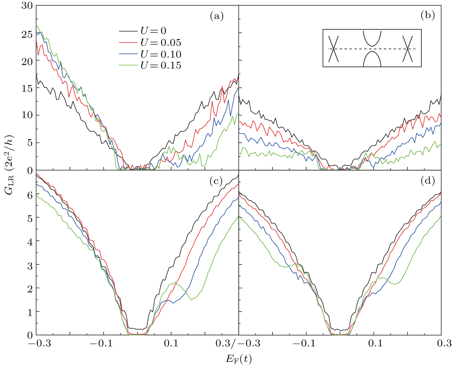
(color online) Plots of conductance versus Fermi energy for different values of bias potential U = 0.00, 0.05, 0.10, 0.15. Panels (a) and (c) correspond to the bottom–bottom configuration with the values of disorder strength W = 0 and W = 1.2. Panels (b) and (d) correspond to the bottom–top configuration under W = 0 and W = 1.2. The other parameters are . The inset shows the corresponding band structures in the three parts.