Direct measurements of conductivity and mobility in millimeter-sized single-crystalline graphene via van der Pauw geometry
Ma Rui-Song1, 2, 3, Huan Qing1, 2, 3, Wu Liang-Mei1, 2, 3, Yan Jia-Hao1, 2, 3, Zhang Yu-Yang2, Bao Li-Hong1, 2, 3, †, Liu Yun-Qi4, Du Shi-Xuan1, 2, 3, Gao Hong-Jun1, 2, 3, ‡
       

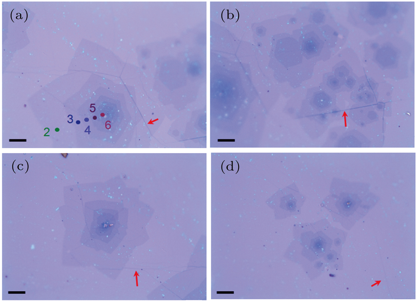
(color online) Optical micrographs of small multi-layered graphene flakes. (a) and (b): Zoom-in optical micrographs showing the multilayers pointed by the left blue arrow in Fig. 2(a). The circles in panel (a) indicate the positions where the Raman spectra in Fig. 2(b) are collected. (c) and (d): Magnified optical images of graphene multilayers indicated by the middle and right blue arrow in Fig. 2(a), respectively. Graphene wrinkles indicated by red arrows can also be found in these optical images. Scale bar: 20 µm.