Direct measurements of conductivity and mobility in millimeter-sized single-crystalline graphene via van der Pauw geometry
Ma Rui-Song1, 2, 3, Huan Qing1, 2, 3, Wu Liang-Mei1, 2, 3, Yan Jia-Hao1, 2, 3, Zhang Yu-Yang2, Bao Li-Hong1, 2, 3, †, Liu Yun-Qi4, Du Shi-Xuan1, 2, 3, Gao Hong-Jun1, 2, 3, ‡
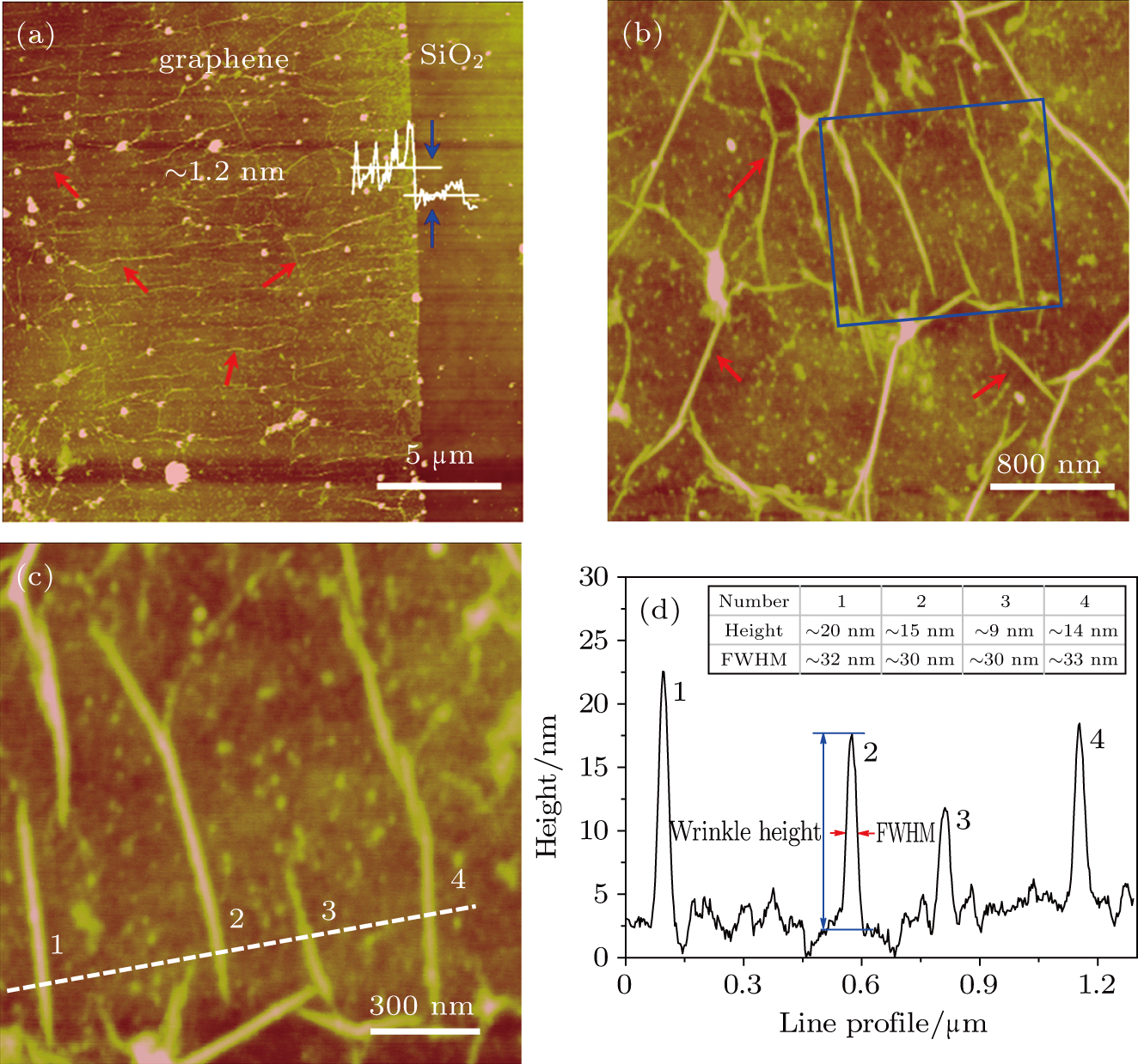
(color online) AFM characterization of graphene on SiO2/Si. (a): AFM height image of the graphene flake shown in Fig. 2. The graphene edge can be identified and the line profile reveals the thickness of this transferred graphene flake to be about 1.2 nm. Wrinkles indicated by red arrows can be found in this transferred graphene. (b): AFM image of the region near the center of the same graphene flake. (c): Magnified AFM image of the region indicated by a blue square in panel (b). (d): Line profile of the graphene wrinkles along the dash line shown in panel (c). The height and full width at half maximum (FWHM) of four wrinkles numbered in panel (c) are summarized in the inset table.