Direct measurements of conductivity and mobility in millimeter-sized single-crystalline graphene via van der Pauw geometry
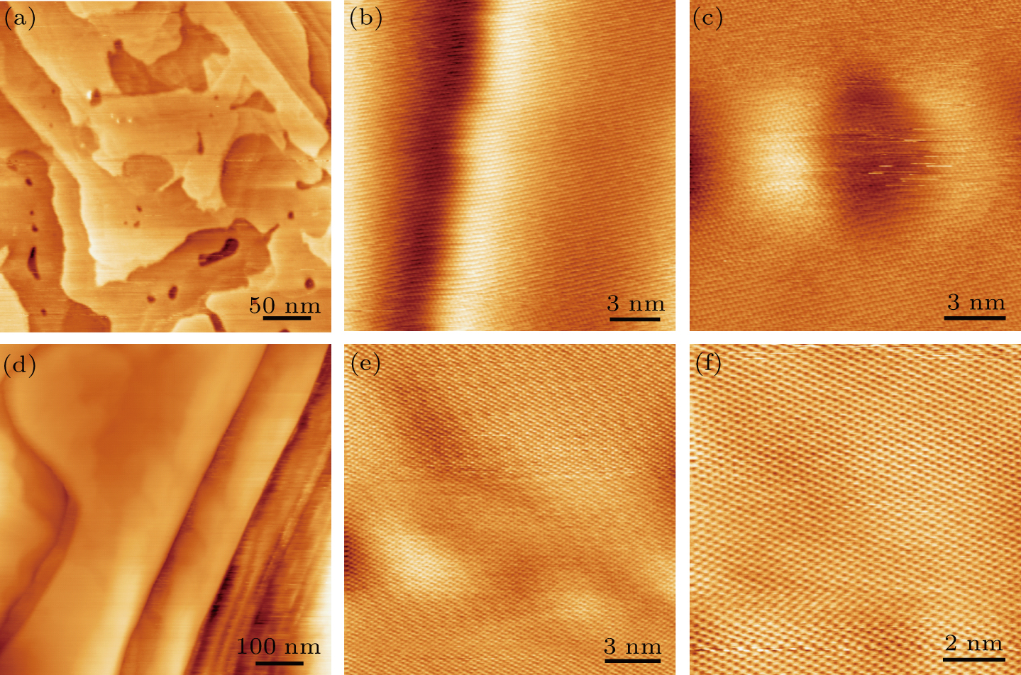
(color online) STM characterizations of graphene on other structures in Cu foil. (a): STM topographic image of one typical structure on Cu foil. Irregular steps with complex shapes and small pits can be revealed in this image. (b): Atomic-scale STM image of graphene across a step in panel (a). (c): Atomic-scale STM image around a pit in panel (a). (d): Large-scale STM image of other structures on Cu foil. (e)–(f): Atomically-resolved STM images on the flat area in panel (d). Honeycomb structures can be clearly resolved in panel (f). The continuities of defect-free graphene lattices shown in panels (b), (c), (e), and (f) also verify the continuity and high quality of the sample. Scanning conditions: (a): It = 300 pA and Vsample = 60 mV. (b) and (c): It = 520 pA and Vsample = 60 mV. (d): It = 358.6 pA and Vsample = 87.16 mV. (e)–(f): It = 823.9 pA and Vsample = 89.12 mV.
