Direct measurements of conductivity and mobility in millimeter-sized single-crystalline graphene via van der Pauw geometry
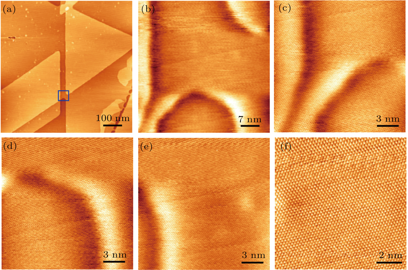
(color online) STM characterization of graphene on Cu foil. (a): Large-area STM image on Cu foil. Parallelogram and triangular structures can be seen in this image. (b): Zoom-in STM image of the area indicated by a blue square in panel (a). (c)–(f): Atomically-resolved STM images within the region shown in panel (b). The triangular structures of graphene lattices are found to cover the fluctuant Cu surface continuously without any defect. These images verify the continuity and high quality of graphene grown on Cu foil. Scanning conditions: (a)–(f) It = 369.4 pA and Vsample = 314.8 mV.
