Direct measurements of conductivity and mobility in millimeter-sized single-crystalline graphene via van der Pauw geometry
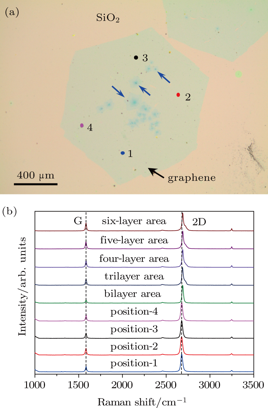
(color online) Optical and Raman characterization of monolayer graphene transferred onto SiO2/Si substrate. (a): Optical micrograph of a monolayer graphene flake on SiO2/Si. Small multilayer flakes indicated by blue arrows are distributed randomly on this millimeter-sized graphene flake. (b): Raman spectra collected on four monolayer positions and multilayers of this graphene flake. The four monolayer positions are indicated by four numbered circles in panel (a) and the positions collected on multilayers are shown in Fig.
