Direct measurements of conductivity and mobility in millimeter-sized single-crystalline graphene via van der Pauw geometry
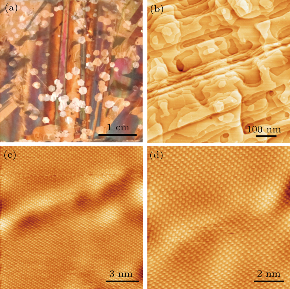
(color online) Optical and STM characterization of graphene grown on Cu foil. (a): Optical photograph of graphene grown on Cu foil by CVD method. The scale bar is 1 cm and the grain size of the graphene grain is in the range of millimeter. (b): STM image showing one of the graphene-covered Cu foil. (c)–(d): Atomically-resolved STM images on the morphology in panel (b). Scanning conditions, (b)–(d): It = 367.3 pA and Vsample = 82.02 mV.
