Design of tunable surface mode waveguide based on photonic crystal composite structure using organic liquid
Zhang Lan-Lan1, †, Liu Wei1, Li Ping1, Yang Xi1, Cao Xu2
School of Medical Technology and Engineering, Henan University of Science and Technology, Luoyang 471000, China
Basic Teaching and Research Section, People’s Liberation Army Rocket Force 96520, Luoyang 471000, China


† Corresponding author. E-mail: zhanglan80515@163.com

Abstract

With the method of replacing the surface layer of photonic crystal with tubes, a novel photonic crystal composite structure used as a tunable surface mode waveguide is designed. The tubes support tunable surface states. The tunable propagation capabilities of the structure are investigated by using the finite-difference time-domain. Simulation results show that the beam transmission distributions of the composite structure are sensitive to the frequency range of incident light and the surface morphology which can be modified by filling the tubes with different organic liquids. By adjusting the filler in tubes, the T-shaped, Y-shaped, and L-shaped propagations can be realized. The property can be applied to the tunable surface mode waveguide. Compared with a traditional single function photonic crystal waveguide, our designed structure not only has a small size, but also is a tunable device.

1. Introduction

Photonic crystals have aroused a great deal of interest recently due to their potential ability to control the propagation of light. They possess many unique physical properties. One of the most unique properties is the existence of a photonic crystal bandgap. Many optical devices based on a two-dimensional (2D) photonic crystal with photonic crystal bandgap have been proposed and they are expected to play important roles in future photonic circuits. The waveguide is one of the indispensable components in these devices. By introducing line defects in photonic crystals, a waveguide can be realized, where light is guided along the line defects. These types of photonic crystal waveguides can be called line defect photonic crystal waveguides. A great amount of study has been conducted in designing photonic crystal line defect waveguides, for example, the T-shaped waveguide, Y-shaped waveguide,[1] and L-shaped waveguide.[2]

Another unique feature of photonic crystal is the surface wave. The surface waves are electromagnetic waves localized at the interface between a photonic crystal and another medium. The introduction of line defects along the photonic crystal surface may lead to the occurrence of surface modes which are different from waveguide guided modes. Waveguide guided modes can appear when the photonic crystal has one or more line defects within its lattice. The surface modes at the photonic crystal-air interface are called the uncoupled surface modes. Surface modes may also appear at the interface between two photonic crystals with modified surface. The surface modes at photonic crystal-photonic crystal interface are called the coupled surface modes.[3] These two photonic crystals can be the same or different. The distance between the two modified photonic crystals can be lattice constant or not lattice constant. For a 2D photonic crystal the existence of surface modes has been shown theoretically and experimentally. Many optical devices based on a photonic crystal surface wave have also been proposed.[4] The original surface waves are of the non-radiative mode, which can only propagate strictly along the surface of photonic crystal and cannot couple to the outside space. For that reason, non-radiative surface modes are regarded as an undesirable feature. Most of the previous work has focused on the physics of surface waves and the radiative surface modes. It has been shown that with the help of radiative surface modes it is possible to achieve a directional beam from the waveguide.[59] Recently, an approach to waveguide design has suggested the possibility of using non-radiative surface wave on the interface boundary between finite photonic crystal and external,[1012] so the interest in non-radiative surface waves in photonic crystals arose again.[1316] The guiding of electromagnetic light waves along the surface boundary of photonic crystal is called photonic crystal surface waveguide.

On the other hand, micro-fluidic devices based on photonic crystals have experienced a significant growth. Many studies have shown the potential application of micro-fluidic devices. For example, Hasek et al. have reported that the sensing of biomaterials is possible in the terahertz region.[17,18] Battula and Chen have reported that a tunable plasmonic-crystal super lens can be designed by using different organic liquids.[19] Chen et al. have reported that a 2D square photonic crystal with the surface modified by tubes can be used to tune beam direction and transmission distribution.[20]

To the best of our knowledge, tunable photonic crystal surface waveguide structures based on composite structure have not been reported so far. In this paper, we propose a novel tunable surface mode waveguide that is based on the non-radiative surface mode. This novel tunable surface mode waveguide structure is a two-photonic-crystal composite structure with the surface modified by tubes. The beam transmission distribution is sensitive to the surface morphology, which can be modified by filling the tubes with different organic liquids. By adjusting the filler in tubes, the T-shaped propagation, Y-shaped propagation, and L-shaped propagation can be realized. Because the transmission distribution is sensitive to the filled liquid, such a kind of structure has an important potential application in integrated optical circuits. It can also be used as micro-fluidic devices to sense micro- and nanoliter volumes of analyte.

2. Structure model and surface mode

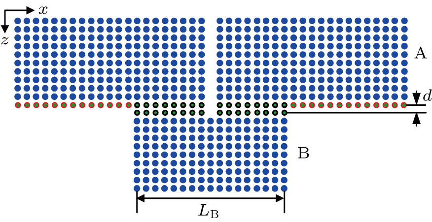
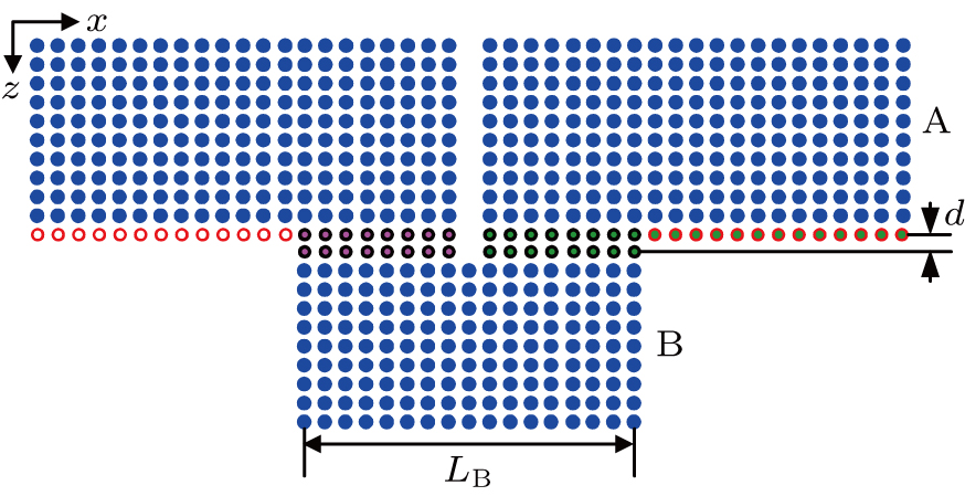
In the present paper, in order to obtain a tunable surface waveguide, we design a novel composition structure as shown in Fig. 1. The structure consists of two photonic crystals (A and B) with a square lattice of dielectric cylinders (denoted by blue dots ) in air. The dielectric constant for each of the cylinders is 11.56 and the radius for each of the dielectric cylinders is r = 0.18a (a is the lattice constant). Photonic crystal A lies above and photonic crystal B lies below photonic crystal A. Photonic crystals A and B have unequal lengths ( and ), with the length of photonic crystal A ( much longer than that of B ( . A waveguide is formed by removing one row of cylinders within photonic crystal A.

Fig. 1. (color online) Schematic diagram of the photonic crystal composite structure. Surface tubes are denoted by black circles and red circles. The outer radius and inner radius of each black circle are 0.16a and 0.1a, respectively; the outer radius and inner radius of each red circle are 0.16a and 0.13a, respectively.

Surface modes can appear at the interface of the photonic crystal-air or photonic crystal-photonic crystal when the surface of photonic crystal is modified. In order to create tunable surface modes, at the input surface of photonic crystal B, the radii of surface cylinders are replaced by the radii of tubes(denoted by black circles) that are made of silicon dioxide (ε = 2.25). The outer radii of these tubes are all 0.16a, and the inner radii 0.1a. At the output surface of photonic crystal A, the radii of surface cylinders are also replaced by the radii of tubes that are madeof silicon dioxide (ε = 2.25). Among these tubes, those tubes (denoted by black circles) that are adjacent to the photonic crystal B each have an outer radius and inner radius 0.16a and 0.1a, respectively. The outer radius and the inner radius of each of the remaining tubes (denoted by red circles) are 0.16a and 0.13a, respectively. These modifications provide the conditions for uncoupled surface modes to exist at the photonic crystal A-air interface and for coupled surface modes to exist at the photonic crystal A-photonic crystal B interface. The distance between the two modified surfaces is d = 0.4a. Photonic crystals A and B constitute a horizontal surface cavity. This horizontal surface cavity is defined as the M cavity, and the length of the M cavity is . Line waveguide divides the M cavity into two cavities: the left cavity and the right cavity.

In the composite structure shown in Fig. 1, there are a line defect waveguide (defined as waveguide A) and two modified interfaces which are located on the output of the photonic crystal A. These two modified interfaces are the photonic crystal A-photonic crystal B interface and the photonic crystal A-air interface. The dispersion relation of the surface mode is sensitive to the surface layer parameters. If we fill the tubes with different organic liquids to obtain different dielectric constants, the dispersion relation of the surface mode can be tuned efficiently. To determine whether the surface modes on the interface with different filled materials exist, we need to calculate the surface wave dispersion relation curves. The curves of surface wave dispersion relation for the photonic crystal A-photonic crystal B interface and the photonic crystal A-air interface shown in Fig. 1 are calculated by using the plane wave expansion (PWM) method[21] together with the super cell approximation method.

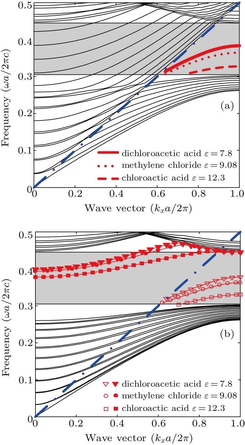
The dispersion relations of uncoupled surface modes (existing at the photonic crystal A-air interface) for surface tubes (denoted by red circles) filled with different organic liquids are calculated, and the results are shown in Fig. 2(a). In this figure, the grey shaded region is the band gap of photonic crystal A for TE mode, whose normalized frequency is in a range of . The blue dash dotted line shows the light line ( determines the light line, where is the momentum parallel to the surface, ω the angular frequency, and c the speed of light). Uncoupled surface modes are denoted by different red curves. They are below the light line, so they are evanescent waves in air; they are in the band gap, so they are evanescent waves in the photonic crystal. So these modes are uncoupled surface modes of the photonic-air interface. We can see that the uncoupled surface mode is very sensitive to the organic liquids. When surface tubes are filled with chloroactic acid (ε = 12.3), the normalized frequency of the surface mode is in a range of . When surface tubes are filled with dichloroacetic acid (ε = 7.8), the normalized frequency of the surface mode is in a range of .

Fig. 2. (color online) Calculated dispersion relation curves of the structure shown in Fig. 1 for surface tubes filled with different organic liquids. (a) Uncoupled surface modes dispersion relation curves, and (b) coupled surface modes dispersion relation curves.

The output surface layer of the photonic crystal A and the input surface layer of the photonic crystal B are modified by a row of tubes. These modifications provide the conditions for coupled surface modes to exist at the interface between photonic crystals A and B. The dispersion relations of coupled surface modes for the surface tubes(denoted by black circles) in the surface layer of the photonic crystal A-photonic crystal B interface, filled with different organic liquids, are calculated, and the results are shown in Fig. 2(b). From this figure, it can be seen that the coupled surface modes of the photonic crystal A–photonic crystal B interface are split into the modes of higher and lower frequencies. The coupled mode with lower frequency has even parity and the one with higher frequency has odd parity with respect to the symmetry plane bisecting the air line between two facing photonic crystals. The coupled even (odd) surface modes are denoted by empty (solid) symbols. One can see from Fig. 2(b) that the coupled surface modes are also very sensitive to the organic liquids. When surface tubes are filled with chloroactic acid (ε = 12.3), the normalized frequencies of even mode and odd mode are in ranges of and , respectively. When surface tubes are filled with dichloroacetic acid (ε = 7.8), the normalized frequencies of even mode and odd mode are in ranges of and , respectively.

3. Simulation results and discussion

In this section, the tunable propagation capabilities of the structure shown in Fig. 1 are studied when surface tubes are filled with different organic liquid. In all the simulations of this paper, the finite-difference time-domain (FDTD) method[22] is employed to numerically calculate the field distributions of the different structures under investigation. The perfectly matched layer boundary conditions are used to surround the computational domain. In all simulations, the Gaussian light source with frequency ω and width a is placed at the line defect waveguide input port. All numerical results presented in this paper are only for the case of TE-polarization (the electric field is perpendicular to the xz plane).

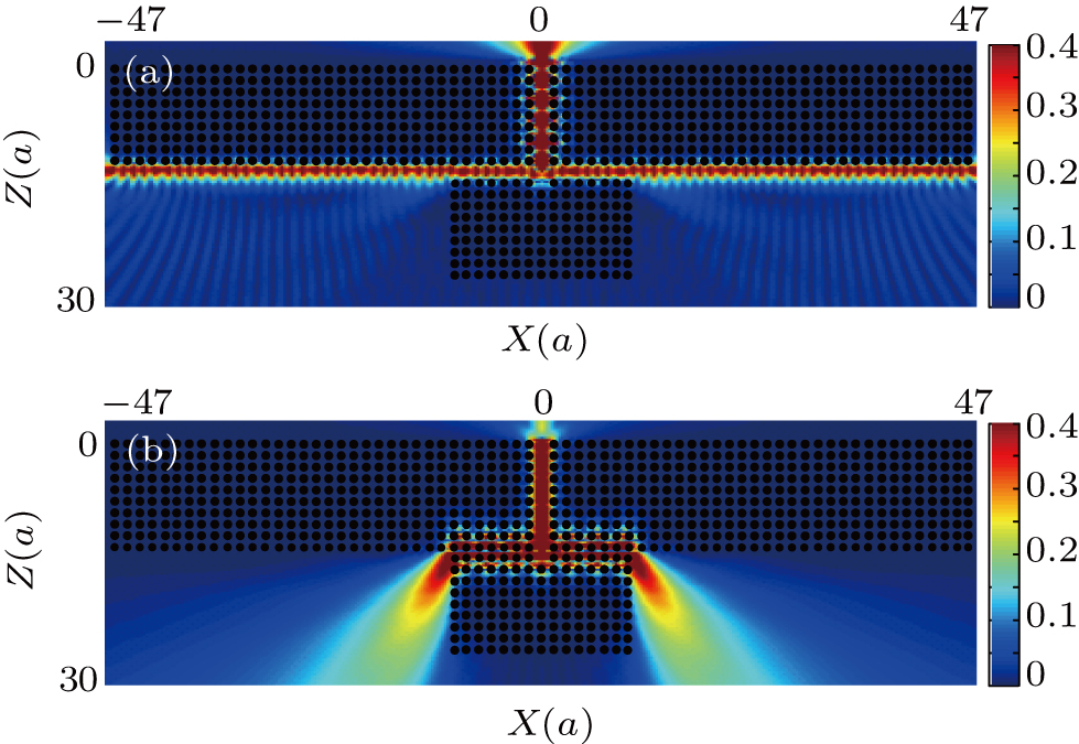
Firstly, in order to obtain T-shaped propagation and Y-shaped propagation, all the surface tubes shown in Fig. 1 are filled with dichloroacetic acid (ε = 7.8) (denoted by green dots). The filled structure is shown in Fig. 3. The field distributions for the corresponding composite structure shown in Fig. 3 are calculated. Figures 4(a) and 4(b) show the calculated spatial distributions when incident beams with two different frequencies, launched at the waveguide input surface, propagate through the waveguide, respectively. Figure 4 indicates that spatial distributions vary with the frequency range of incident beam changing.

Fig. 3. (color online) Schematic diagram of the filled photonic crystal composite structure. All the surface tubes are filled with dichloroacetic acid (ε = 7.8).
Fig. 4. (color online) Simulated spatial distributions of for the structure illustrated in Fig. 3, for (a) and (b) .

Figure 4(a) shows the simulated spatial distribution when the incident wave has a normalized frequency (this frequency is in the overlapping part of the band gap, uncoupled surface mode and even coupled surface mode). From this figure it can be seen that when a plane wave of TE polarization with normalized frequency is incident normally at the waveguide input port, it first propagates along the waveguide. At the exit of waveguide A, the external electric field of the horizontal cavity mainly is distributed at the interface of photonic crystal A-air. The property can be used to design the surface mode photonic crystal T-shaped waveguide. The numerical results presented in Fig. 4(a) can be understood as follows. When the incident source with is placed at the photonic crystal A waveguide input port, it first propagates along the waveguide because it is in the band gap. At the waveguide exit, even coupled surface modes are first excited because the frequency of emission light is also in the frequency range of even coupled surface modes. After an even coupled surface wave travels along the interface between photonic crystals A and B, since uncoupled surface modes are also excited, the coupled surface wave can be coupled out of the M cavity and propagate along the interface of photonic crystal A-air.

Figure 4(b) shows the simulated spatial distribution when incident wave has a normalized frequency (this frequency is in the overlapping part of the band gap and odd coupled surface mode, but excluding the uncoupled surface modes). From this figure, it can be seen that the Y-beam splitting phenomenon can be found. The property can be used to design the surface mode photonic crystal Y-shaped waveguide. The numerical results presented in Fig. 4(b) can be understood as follows. When an incident source with is placed at the photonic crystal A waveguide input port, it first propagates along the waveguide because it is in the band gap. At the waveguide exit, odd coupled surface modes are first excited because the frequency of emission light is also in the frequency range of odd coupled surface modes. After an odd coupled surface wave travels along the interface between photonic crystals A and B, since uncoupled surface modes are not excited, the coupled surface wave can be coupled out of the M cavity and scattered into free space.

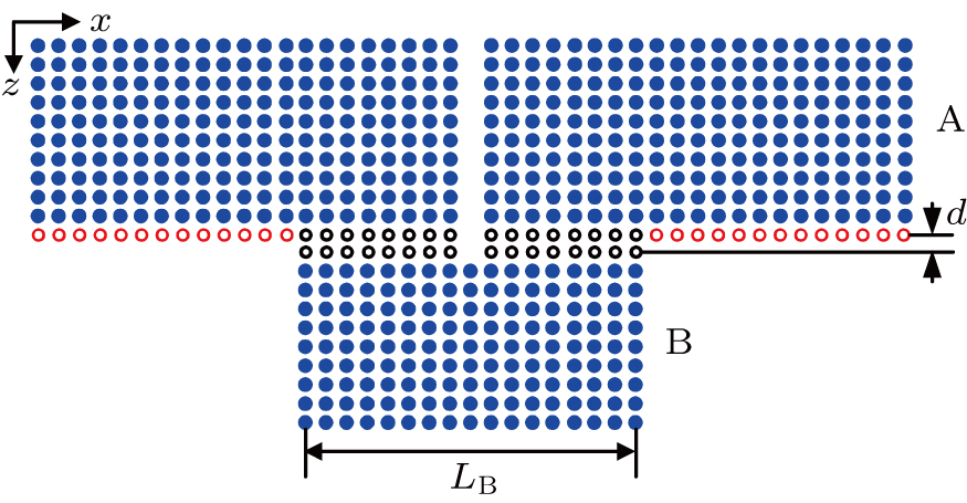
In order to obtain L-shaped propagation, we use different filling methods to fabricate the filled structure as shown in Fig. 5. This filling method is described as follows. The right side output surface tubes of photonic crystal A and the right side input surface tubes of photonic crystal B are filled with dichloroacetic acid (ε = 7.8) (denoted by green dots); the surface tubes which are on the left side of the M cavity are filled with chloroacetic acid (ε = 12.3) (denoted by magenta dots); the left side surface tube which in photonic crystal A-air are not filled with any material. For this filling method, the symmetry of the surface morphology is broken. The purpose of such an asymmetric filling is that the light emitted from waveguide A can excite surface modes at the surface on the right side of photonic crystal A-photonic crystal B but cannot excite surface modes at the left side interface of photonic crystal A-photonic crystal B.

Fig. 5. (color online) Schematic diagram of the photonic crystal composite structure. Right side surface tubes are filled with dichloroacetic acid (green dots); surface tubes on the left side of the M cavity are filled with chloroacetic acid (magenta dots).

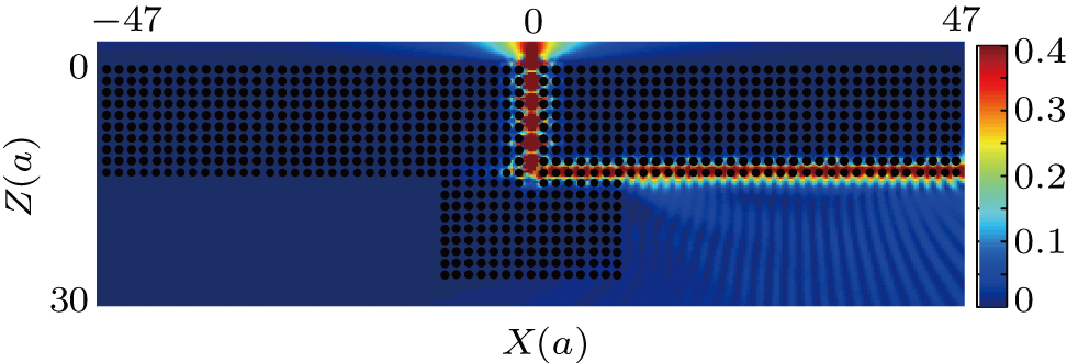
Figure 6 shows the simulated spatial distribution when the normalized frequency of incident is . From this figure it can be seen that an L-shaped propagation phenomenon can be found. The property can be used to design surface mode photonic crystal L-shaped waveguide. The causes of these phenomena shown in Figs. 6 and 4(a) are similar. Their difference is that even coupled surface modes are not excited at the left interface between photonic crystals A and B in Fig. 6, so L-shaped propagation occurs.

Fig. 6. (color online) Simulated spatial distribution of for the structure illustrated in Fig. 5 when .

Figures 4 and 6 show some interesting phenomena. (i) Spatial distributions depend on the frequency of incident light and the materials that are filled in tubes. (ii) The T-shaped propagation and Y-shaped propagation emerge when all the surface tubes shown in Fig. 1 are filled with dichloroacetic acid. (iii) The L-shaped propagation emerges when using the following filling method: the right side surface tubes are filled with dichloroacetic acid, and the surface tubes on the left side in the M cavity are filled with chloroacetic acid and the remaining surface tubes are not filled with any material. Based on these results, novel T-shaped, Y-shaped, and L-shaped surface mode waveguides can be proposed. The property can be applied to tunable surface waveguide structure. Compared with the traditional photonic crystal waveguide structure, our designed waveguide structure has the following advantages: i) the size of our designed waveguide structure is small: the traditional photonic crystal waveguide structure needs two equal width photonic crystals to confine light on both sides of the waveguide; ii) our designed waveguide structure can be used as a multi-function surface mode waveguide, but the traditional photonic crystal waveguide has only a unique waveguide function when the device is fabricated.

In this paper, a novel tunable surface mode waveguide structure is designed. The designed structure consists of a line photonic crystal waveguide and finite photonic crystal. For this proposed device, its fabrication is similar to that of conventional photonic crystal devices, which can be fabricated by electron-beam lithography technology[23,24] and holographic lithography technology.[25] For practical applications, it is very valuable to experimentally verify the theoretical analysis. The techniques reported in the literature provide the basis for the feasibility of the experiment. It is our future work to verify the theoretical analysis experimentally.

4. Conclusions

In this work, we design a new tunable surface waveguide by the method of replacing the surface layer of composite photonic crystal structure with tubes. Using the FDTD method, we obtain the field pattern for several filling forms of the photonic crystal structures. The simulation results show that beam patterns depend on the frequency of incident light and the materials which are filled in surface tubes. The T-shaped propagation and Y-shaped propagation emerge when all the surface tubes are filled with dichloroacetic acid. L-shaped propagation can be realized if the tubes are filled with different fluids in the left and right side of the z axis. The property can be applied to tunable surface waveguide. Compared with a traditional single function photonic crystal waveguide, our design structure not only has a small size, but also is a multifunctional device.

Reference
[1] Boscolo S Midrio M 2002 Opt. Lett. 27 1001
[2] Mekis A Chen J C Kurland I Fan S H Villeneuve P R Joannopoulos J D 1996 Phys. Rev. Lett. 77 3787
[3] Choi H G Oh S S Lee S G Kim M W Kim J E 2006 J. Appl. Phys. 100 123105
[4] Jiang B Zhang Y J Wang Y F Zheng W H 2014 Opt. Commun. 310 114
[5] Lezec H J Degiron A Devaux E Linke R A Martin-Moreno L Garcia-Vidal F J Ebbesen T W 2002 Science 297 820
[6] Jiang L Y Jia W Li H P Li X Y Cong C X Shen Z X 2009 J. Opt. Soc. Am. 26 2157
[7] Moreno E García-Vidal F J Martín-Moreno L 2004 Phys. Rev. 69 121402
[8] Jia W Jiang L Y Chen K Li X Y 2010 Opt. Commun. 283 4078
[9] Wang Q Zhang L L Li Q 2010 Opt. Express 18 24245
[10] Rahachou I Zozoulenko I V 2006 J. Opt. Soc. Am. 23 1679
[11] Khoo E H Cheng T H Liu A Q Li J Pinjala D 2007 Appl. Phys. Lett. 91 171109
[12] Jiang B Zhou W J Chen W Liu A J Zheng W H 2011 J. Opt. Soc. Am. 28 2038
[13] Jiang B Zhang Y J Wang Y F Liu A J Zheng W H 2012 Appl. Opt. 51 2361
[14] Gao Z Gao F Zhang B L 2016 Appl. Phys. Lett. 108 041105
[15] Hu J X Fang Y T 2015 Int. J. Mod. Phys. 29 1550159
[16] Erim M N Erim N Kurt H 2013 Photon. Nano. Fund. Appl. 11 123
[17] Hasek T Kurt H Citrin D S Koch M 2006 Appl. Phys. Lett. 89 173508
[18] Kurt H Citrin D S 2005 Appl. Phys. Lett. 87 041108
[19] Battula A Chen S C 2007 Phys. Rev. 76 193408
[20] Chen H B Chen X S Wang J Lu W 2008 Physica 403 4301
[21] Berenger J P 1994 J. Comput. Phys. 114 185
[22] Taflove Hagness S C 2000 Computational Electrodynamics: The Finite-Difference Time-Domain Method Boston Artech House 80 84
[23] Assefa S Petrich G S Kolodziejski L A Mondol Smith H I 2004 J. Vac. Sci. Technol. 22 3363
[24] Xu X S Xiong Z G Sun Z H Du W Lu L Chen H D Jin A Z Zhang D Z 2006 Acta Phys. Sin. 55 12481 in Chinese
[25] Liu H Yao J Q Li E B 2006 Acta Phys. Sin. 55 2286 in Chinese