1. IntroductionIn the past few decades, the surface plasmon resonances (SPRs) and surface plasmon polarities (SPPs) in noble metal nanoparticles and nanostructures have been widely studied because of their tremendous potential applications in light harvesting,[1] nanolaser,[2] and surface enhanced spectroscopy.[3] Recently, it was also found that the surface plasmons (SPs) of metal nanoparticles can be used to enhance or control the absorption and photoluminescence of some two-dimensional materials.[4,5] The SP responses of metal nanostructures are sensitive to the environment accompanied with high electromagnetic field enhancements, which lead to extensive researches on plasmonic sensors.[6–12] In particular, refractive index (RI) sensors based on SP responses can achieve the label-free and real time detection, and have received a great deal of attention.[6–11]
Recently, SP responses in the ultraviolet (UV) region have aroused considerable interest because the high photon energies can match electronic transition energies of many organic molecules and photoelectric materials.[13] It is well known that the SP resonances of Au or Ag cannot extend into the deep UV region. Aluminum is an alternative candidate with SP responses in the deep UV region, which also has the advantages in low cost, high natural abundance, and ease of processing.[13] Therefore, Al nanoparticles and nanostructures have been considered for many promising applications in the UV region such as light harvesting,[14] surface enhanced spectrum,[15] and sensing.[8–11] Norek et al.[9] and Cheng et al.[10] have demonstrated the UV RI sensors based on the SPRs of Al pit arrays. However, strong scattering and intrinsic damping of the metal elements will introduce great loss and hence broaden the resonances, which is unfavorable for RI sensing. Setting dielectric structures on the metal surface can excite and control SPPs (so-called dielectric loaded surface plasmon polaritons (DLSPPs)).[16] Fang et al. have demonstrated experimentally the excitation of DLSPPs by placing a CdS nanostripe on an Ag layer, which avoids the intrinsic losses of metal elements and results in sharp resonances.[17] Therefore, DLSPPs have been widely used in light sources,[18] light focusing,[19,20] light harvesting,[21] superlens,[22] light couplers, and splitters.[23,24]
In this paper, we investigate the DLSPP properties of an Al
 O
O
 –Al nanostructure by using the finite element method (FEM). This nanostructure is composed of an aluminum film covered with a dielectric grating. The DLSPPs of the Al
 O
O
 –Al nanostructure lead to sharp SP responses in the deep UV. The influences of the element height, grating period, and filling factor on the DLSPPs are studied systematically. We further find that the DLSPPs in the Al
 O
O
 –Al nanostructure are sensitive to the environment and hence it could be utilized as a UV refractive index sensor.
2. The Al
 O
O
 –Al nanostructure
The Al
 O
O
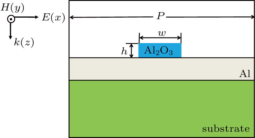
 –Al nanostructure is depicted in Fig. 1. An Al
 O
O
 grating is set to be on an Al film. The Al film on the substrate is 100 nm thick throughout the study, enough to eliminate direct light transmission. The height and width of the Al
 O
O
 element are h and w, respectively. The period of the grating is P and the filling factor f is defined as w/P. The dielectric grating is infinite along the y axis. To excite SPPs on the upside of the metal film, the electric field of the incident light is polarized along the x axis and the propagation vector is parallel to the z axis. The periodic boundary condition is used at boundaries orthogonal to the x axis. Although the incident light should be a little oblique to split from the reflected light in experiments, the angle is so small that people usually consider the normal incidence.[6]
The reflection spectra of the structure are calculated by using the 2D-FEM. The FEM has been proved to be a flexible and efficient numerical tool to study the optical properties of nanostructures.[25] To avoid nonphysical reflections of the outgoing electromagnetic waves from boundaries, perfectly matched layers are used at the top and bottom boundaries. The permittivity parameters of Al, Al
 O
O
 , and the embedding medium are
 ,
,
 , and
, and
 , respectively. The value of
 is fixed at 3.24,[26] and
 can be described by the Drude model based on the experimental data as follows:[27]
where the bulk plasma frequency

eV and the bulk collision frequency

eV. Generally, the quality of the RI sensor is evaluated by the sensitivity

and the figure of merit FOM =
S/FWHM, where

is the spectrum change of the resonance induced by the refractive change

, and FWHM stands for full width at half maximum and here it refers to the line width of the resonance.
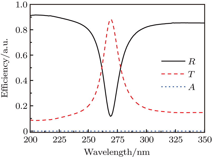
3. Results and discussionIn Fig. 2, the solid, dotted, and dash lines show the reflection (R), transmission (T), and absorption (A = 1 − R − T) spectra of the Al
 O
O
 –Al nanostructure, respectively. Here, the height h of the grating element is fixed at 50 nm, the grating period P is 150 nm, and the filling factor
 . The surrounding material is water (
 .
.
The transmission T of the structure is nearly zero. In the reflection spectrum, a strong dip can be observed at around 270 nm. As the light irradiates on the Al
 O
O
 grating normally, diffractions in the grating provide the wave vector conservation. SPPs are excited and propagate on the metal surface. When the distance between the grating elements is a multiple of the SPP wavelength, SPPs interfere constructively and most of the incident light energy is transferred into them.[28,29] Therefore, a reflection dip occurs in the reflection spectrum. Because the surface waves are excited by dielectric elements, they are referred to as DLSPPs. The dielectric elements avoid inherent metal loss and hence the FWHM of the SP response is only about 15 nm. Such a small FWHM is preferred for realizing the high quality RI sensing.
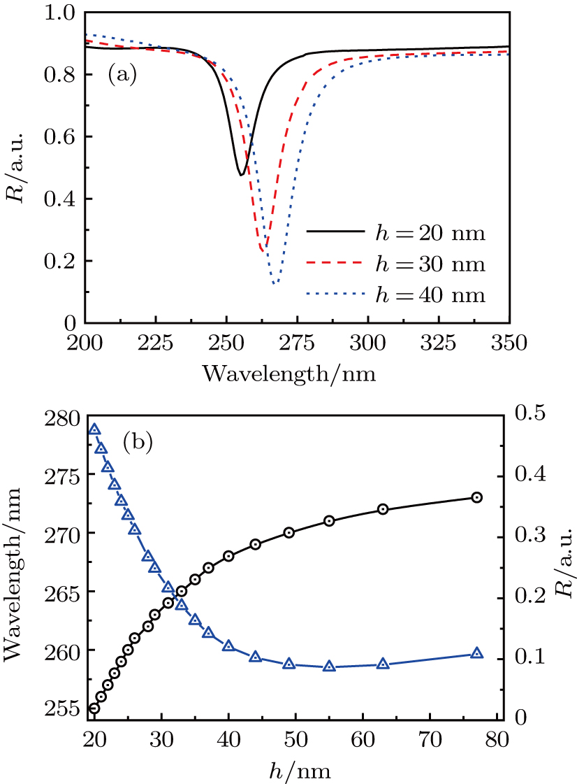
Second, we will study the influence of the height h of the grating element on the optical properties of the Al
 O
O
 –Al nanostructure. In Fig. 3(a), the solid, dash, and dotted lines show the reflection spectra of the Al
 O
O
 –Al nanostructure with h values of 20, 30, and 40 nm, respectively. Here, P and f are fixed at 150 nm and 0.5, respectively. It is found that with increasing the h value, the reflection spectrum of the Al
 O
O
 –Al nanostructure shows a distinct red-shift while the reflection dip becomes deeper. The increased h will modify the phase of SPP wave and then leads to the redshift of the reflection dip.[20,29] Since the dielectric elements will not absorb the incident light, the deeper reflection dip means more incident light can be transferred into SPPs. With the increase of the h value, the periodic perturbation above the metal film becomes stronger and hence more incident light couples into SPPs.
In Fig. 3(b), the circle-dash line for the left-hand scale and the triangle-dash line for the right-hand scale show the resonant wavelength and the minimal reflection of the Al
 O
O
 –Al nanostructure, each as a function of the h value, respectively. As h < 45 nm, with increasing the h value, the reflection dip is red-shifted and falls down quickly. As h > 45 nm, further increase of the h value leads to very weak changes in the reflection spectra.
In the Al
 O
O
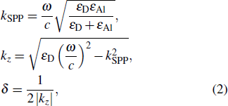
 –Al nanostructure, DLSPPs propagate on the interface between Al and the surrounding medium or the dielectric elements alternatively.[19,29] They decay quickly in the direction normal to the surface. The penetrating length δ in the dielectric material can be estimated from the following equations:[28]
where

is the wave number of SPP waves,
ω is the angular frequency of the incident light,
c is the velocity of light in free space, and

is the permittivity of the dielectric material. If

, the change of the
h value will induce negligible variation in the DLSPP. According to Eq. (
2), the
δ value of the Al

O

–Al interface is smaller than 45 nm in the UV region (wavelength from 200 nm to 400 nm). Thus, as

nm, the reflection spectrum of the Al

O

–Al nanostructure rarely changes with the
h value. These results are consistent with the results of previous researches.
[29]We will further investigate the effects of the lattice parameter P and the filling factor f on the optical response of the Al
 O
O
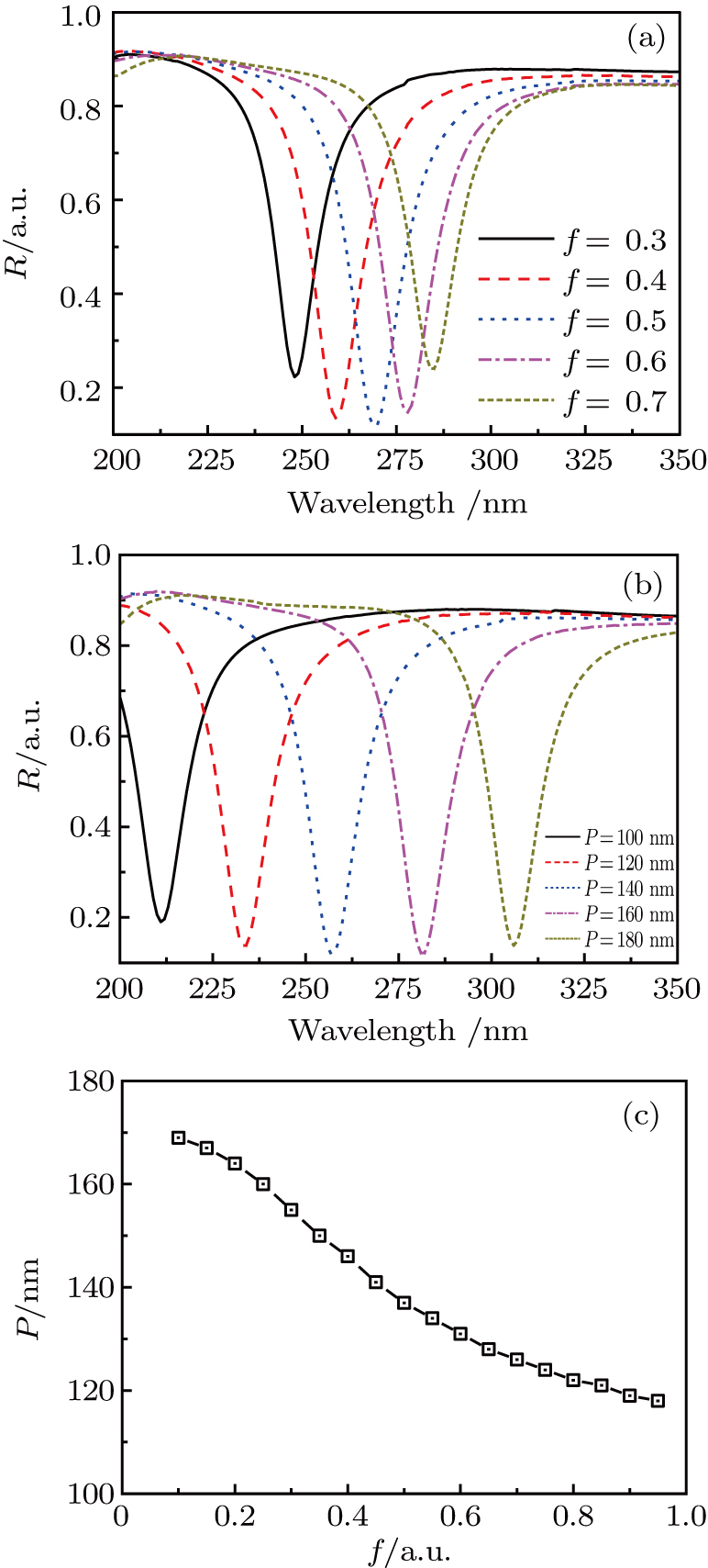
 –Al nanostructure. In the following investigations, the h-value is fixed at 50 nm to make sure that the SP responses will not be affected by h. In Fig. 4(a), the solid, dash, dotted, dash-dotted, and short dash lines represent reflection spectra of the Al
 O
O
 –Al nanostructure with f-values of 0.3, 0.4, 0.5, 0.6, and 0.7, respectively. Here, P is fixed at 150 nm. It is found that the reflection spectrum shows a redshift with the increase of f value. The increased filling factor will increase the effective refractive index above the metal and hence results in the redshift of the DLSPP resonance.[29]
In Fig. 4(b), the solid, dash, dotted, dash-dotted, and short dash lines represent reflection spectra of the Al
 O
O
 –Al nanostructure with P values of 100, 120, 140, 160, and 180 nm, respectively. Here,
 and h = 50 nm. The reflection spectrum of the Al
 O
O
 –Al nanostructure also shows a distinct redshift with the increase of the P value. According to the surface plasmon diffraction theory,[19,28] the reciprocal lattice vector
 provides the
 under normal incidence. The increased P value will reduce the
 value. Then, from Eq. (2), the corresponding ω-value decreases and hence the DLSPP resonance of the Al
 O
O
 –Al nanostructure is red-shifted. Therefore, the position of the reflection dip of the Al
 O
O
 –Al nanostructure can be modulated by changing the lattice parameter P and the filling factor f. This means that we can find many groups of P and f for realizing resonances at some specific wavelengths. Figure 4(c) shows the variation of the P-value as a function of the f value for achieving the reflection dip at 254 nm. It is well known that many hydrocarbons are sensitive to the irradiation at 254 nm and photons at this wavelength are also important for light cleaning.[30,31] To ensure the DLSPP resonance at 254 nm, the P value decreases with the increase of the f value.
Finally, we study the RI sensing properties of the Al
 O
O
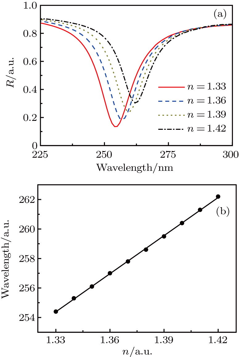
 –Al nanostructure. The initial working wavelength is assumed to be 254 nm. Figure 5(a) shows the reflection spectra of the RI sensor in diffident surrounding media. Here, f = 0.4, h = 50 nm, and P = 146 nm. The solid, dash, dotted, and dash-dotted lines represent the reflection spectra for n-values (where
 ) of 1.33, 1.36, 1.39, and 1.42, respectively. With increasing the n-value, the reflection dip shows a distinct redshift from about 254 nm for
 to about 262 nm for n = 1.42. Through the linear fitting as shown in Fig. 5(b), we can obtain that the sensitivity S of this UV RI sensor is about 86 nm/RIU, and the corresponding FOM is about 5.73. The obtained sensitivity S of the Al
 O
O
 –Al nanostructure is smaller than those of the reported UV RI sensors based on Al pit arrays.[9,10] However, the FOM of the Al
 O
O
 –Al nanostructure is much better than those of these previous researches. This is because the DLSPPs of the Al
 O
O
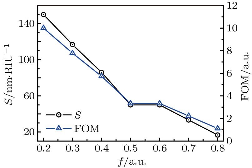
 –Al nanostructure can avoid the inherent metal loss and hence the FWHM of the SP response is only about 15 nm. As a comparison, the SP resonances of the reported Al pit arrays span about 100 nm. Figure 6 shows the S and FOM of the Al
 O
O
 –Al nanostructure, each as a function of f value. The height of the grating element is fixed at 50 nm. The initial working wavelength of the UV RI sensor is set to be 254 nm. It is found that the S and FOM both vary almost inversely with the f value. The reduced f value will increase the detecting area and hence result in the increases of S value and FOM value.


