Fabrication of crystalline selenium microwire
Peng Shuai1, 2, 3, Tang Guo-Wu1, 2, 3, Sun Min1, 2, 3, Liu Wang-Wang1, 2, 3, Shan Xiu-Jie1, 2, 3, Qian Qi1, 2, 3, †, Chen Dong-Dan1, 2, 3, Zhang Qin-Yuan1, 2, 3, Yang Zhong-Min1, 2, 3
State Key Laboratory of Luminescent Materials and Devices and Institute of Optical Communication Materials, South China University of Technology, Guangzhou 510640, China
Guangdong Engineering Technology Research and Development Center of Special Optical Fiber Materials and Devices, South China University of Technology, Guangzhou 510640, China
Guangdong Provincial Key Laboratory of Fiber Laser Materials and Applied Techniques, South China University of Technology, Guangzhou 510640, China


† Corresponding author. E-mail: qianqi@scut.edu.cn

Abstract

A method of fabricating selenium (Se) microwire is demonstrated. A multimaterial fiber with amorphous selenium (a-Se) core and multicomponent phosphate glass cladding is drawn by using a conventional optical fiber drawing technique. Then the a-Se core of the fiber is crystallized by a post thermal process at 150 °C. After the multicomponent phosphate glass cladding is stripped from the multimaterial fiber by marinating the fiber in HF acid solution, a crystalline selenium (c-Se) microwire with high uniformity and smooth surface is obtained. Based on microstructure measurements, the c-Se microwire is identified to consist of most hexagonal state particles and very few trigonal state whiskers. The good photoconduction property of c-Se microwire with high quality and longer continuous length makes it possible to apply to functional devices and arrays.

1. Introduction

In recent years, crystalline semiconductor filaments have received increasing attention due to their unique physical properties and potential for a wide range of applications such as future electronic and optoelectronic devices.[14] Several methods have been employed to fabricate microwires and nanowires including vapor–liquid–solid (VLS) growth,[5] high pressure chemical vapor deposition (HPCVD),[6] solution–liquid–solid approach,[7] and solid–solution–solid growth process.[8] The conventional VLS has been an important approach to the fabrication of high-quality microwires and nanowires. Nevertheless, filaments produced by this approach are limited to the mechanical fragility and lack of global orientation.[9] For the HPCVD method, currently it is impossible to achieve long lengths of microwires because of its slow deposition rate.[10] The other methods described above are inconvenient to produce crystalline structure microwires.

Selenium is an important semiconductor with unique properties, such as high photoconductivity, large piezoelectric, thermoelectric effect and nonlinear optical response.[11] Therefore, Se microwires show great potential applications in electronic, optical electronic devices and starting materials for fabricating the other functional materials.[12,13] Here a method to fabricate crystalline Se microwire by using a conventional optical fiber drawing technique is provided. This process has unique advantages: it takes full advantage of the fundamental simplicity of the traditional fiber drawing process and allows longer continuous lengths of c-Se microwires with high uniformity and smooth surface to be readily realized.

2. Experimental details

Commercial Se powder of 99.9% purity was prepared to fill in an 8-cm-long self-developed multicomponent phosphate glass (55P O -18K O-13BaO-14Al O wt%) tube with an outer diameter of about 28 mm and inner diameter of 3 mm, under vacuum condition. After sealing the two ends of the cladding glass tube, the tube was drawn into fiber in an argon atmosphere at approximately 660 °C. In order to crystallize Se core, the as-drawn Se core fiber was then annealed by a post-thermal process at 150 °C for 1 h.

The cross section and section of the obtained multimaterial fiber with Se core and multicomponent phosphate glass cladding were observed by optical microscope (OM, Olympus). Then the fiber samples were etched in HF acid (50% in deionized water) for two hours to dissolve glass cladding and obtain Se microwires. Microstructural analysis and the distribution of elements were investigated by using a Nova Nano SEM1530 scanning electron microscope with an energy dispersive x-ray spectrometer (EDS). The surface of the c-Se microwire was observed by using a Bruker Multimode 8 Atomic force microscopy (AFM). To determine the structure and crystal phase of the microwire, high-resolution transmission electron microscopy (HR-TEM) images and selected area electron diffraction (SAED) patterns were obtained by transmission electron microscope (TEM, JEM-2100F). The photosensitive current of the fibers between dark and illuminated states (under illumination from 532-nm DPSS laser, 632-nm HeNe laser and 808-nm HeNe laser) were recorded by using Keithley series 2450 source meter. All measurements were made at room temperature.

3. Results and discussion

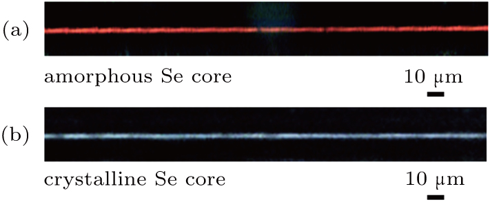
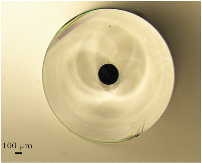
The topography of the as-drawn multimaterial fiber is shown in Fig. 1. Based on the scale bar in Fig. 1, the outer and core diameter of the multimaterial fiber are 1.7 mm and 300 μm, respectively. Figures 2(a) and 2(b) show a fiber section having a brick-red characteristic amorphous selenium and a dark-gray characteristic crystalline selenium, respectively.[9] The transition of the selenium core in the fiber from amorphous state to the crystalline state can be readily discerned visually from the dramatic change in selenium core color. Upon drawing the fiber, the fiber rapidly cooling results in the Se core quenching into the amorphous Se. Because the Se core of as-drawn fiber is unstable and can easily go between amorphous and crystalline states, the a-Se core can be converted into the equilibrium crystalline Se (c-Se) simply by a post-thermal process at 150 °C for 1 h.[14,15] This treatment temperature is substantially below the cladding phosphate glass transition temperature ( ∼ 480 °C),[16] so the glass cladding was unaffected by the annealing.

Fig. 1. (color online) (a) Optical micrograph image of the cross section of a-Se core fiber.
Fig. 2. (color online) (a) Optical micrograph image of a-Se core fiber. (b) Optical micrograph image of c-Se core fiber annealing at 150 °C for 1 h.

To obtain net c-Se microwire, it is necessary to strip the multicomponent phosphate glass cladding from the multimaterial fiber. Because this multicomponent phosphate glass is prone to dissolving in HF solution while selenium is not, c-Se microwires are obtained by marinating the fibers in HF acid (50% in deionized water) for two hours. The SEM image of the c-Se microwire in the inset of Fig. 3(a) shows that its diameter is about 300 μm, which is in accordance with the core diameter observed from Fig. 1 and verifies that selenium does not dissolve in the HF acid solution. The EDS spectrum in Fig. 3(a) shows that only Se and Pt elements are observed in the microwire sample. Elemental Pt comes from the platinum sputtering treatment on the sample for SEM and EDS observation, so the microwire can be identified to be composed of net Se.
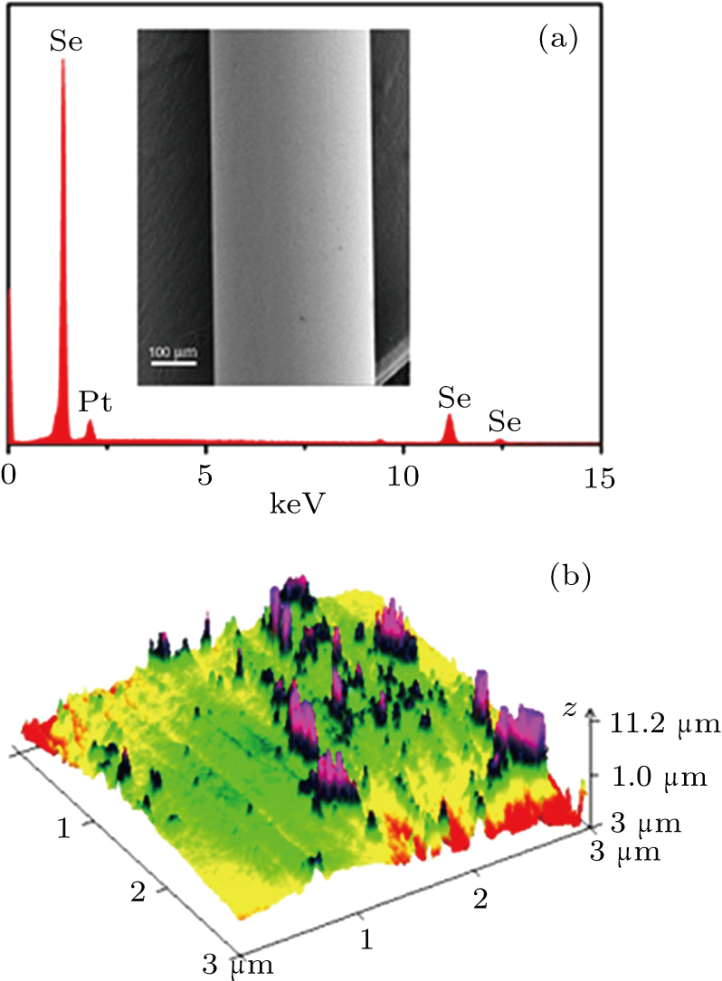
Fig. 3. (color online) (a) Elemental analysis image of c-Se microwire, the inset showing the SEM image of the microwire. (b) The AFM image of c-Se microwire.

The surface roughness of microwire has a remarkable effect on combined microstructure of microwires and wave guide transmission loss due to surface scattering.[17,18] An AFM surface image of the c-Se microwire is observed with a Z direction resolution of 0.01-nm RMS as shown in Fig. 3(b). The AFM data are analyzed by using nanoscope analysis freeware, and the root-mean-square roughness of the c-Se microwire is approximately 1.95 nm. It has been reported that as surface roughness was less than 4 nm, the surface scattering of microwire did not contribute significantly to transmission loss.[18] This implies that the c-Se microwire with more smooth surface will result in low loss, which is advantageous for nonlinear optics or optoelectronic applications. Based on these results above, therefore, it should not be surprising that the current method of fabricating c-Se microwire allows good quality and longer continuous lengths of c-Se microwire to be simply realized.

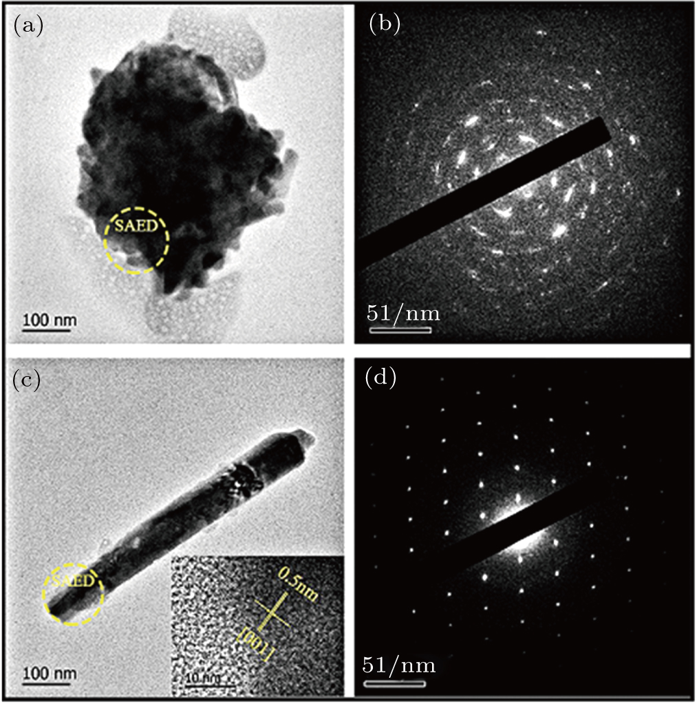
To further study the microstructure of the c-Se microwire, the c-Se microwire is crushed, then the TEM, SAED, and HR-TEM measurements are performed. Some Se particles can be observed from the TEM image in Fig. 4(a). The SAED image of the selected area (yellow circle) in Fig. 4(a) is shown in Fig. 4(b). This SAED pattern has a polycrystalline character, indicating that the microwire is composed of Se crystal particles. A whisker, coming from the crushed c-Se microwire, is observed in TEM image of Fig. 4(c) and the selected area (yellow circle) is about 130 nm in diameter. The SAED pattern shown in Fig. 4(d) reveals that the 130-nm area of whisker is occupied by single crystalline body. The HR-TEM image in the inset of Fig. 4(c) demonstrates that a crystal lattice fringe spacing of the whisker is ∼ 0.5 nm, which agrees well with the separation of the (001) crystal facet of the trigonal phase Se.[19] It is well known that trigonal-Se is apt to grow into 1D structure because of its unique atom chains, which favors anisotropic growth.[19] However, the c-Se microwire has been identified to be hexagonal phase by the XRD measurement.[20] This may result from the content of trigonal phase Se in c-Se microwire being lower than the detection limit of XRD. Therefore, it seems that this c-Se microwire consists of mostly hexagonal Se particles with a small quantity of trigonal phase whiskers.

Fig. 4. (color online) (a) and (c) TEM images of the c-Se microwire powder. (b) and (d) SAED patterns of the selected area (yellow circle) of the c-Se microwire powder in panels (a) and (c), respectively. The inset of Fig. 4(c) shows the HR-TEM image of a-Se whisker in panel (c).

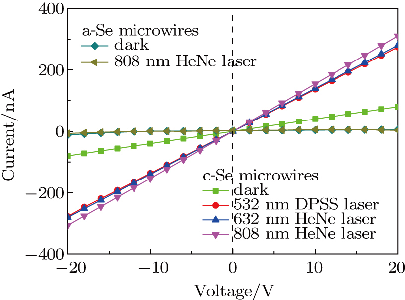
Photoconduction is an important characterization for a crystalline semiconductor microwire and it has been reported that there are some changes in conductivity between dark and illuminated states in semiconductor core fibers.[20,21] To study the photoelectric properties of Se microwire, 1cm-long a-Se and c-Se microwires are directly connected to external circuitry. Figure 5 shows the voltage–current plots of the two microwires under dark state and these states illuminated by 532-nm DPSS laser, 632-nm HeNe laser, and 808-nm HeNe laser, at the same energy density of 200 mW/cm , respectively. As is observed, no currents in the a-Se microwire are observed under dark state nor illuminated state due to its extremely low conductivity ( ).[9,21] Meanwhile, for the c-Se microwire, some remarkable current changes can be observed between dark and illuminated states. The calculated conductivity of the c-Se microwire in the dark is much less than that of bulk single crystal Se (10 cm ), which may be attributed to the reflection of electrons at grain boundaries or defects along the high aspect ratio filaments.[22] The largest difference with over three times the change in conductivity between the dark (1.6 × 10 cm ) and the illuminated states under 808-nm HeNe laser (6.0 × 10 cm ) suggest that the c-Se microwire may have promising utility in photodetectors and optical switches. The different conductivities under three illuminating wavelengths, although their difference values are small, show that c-Se microwire is more sensitive to 808-nm laser illuminated than at 532 nm or 632 nm. This arises from the fact that the longer wavelength of laser illumination can result in less grain boundary scattering in the polycrystalline Se microwire.

Fig. 5. (color online) Current–voltage characteristics of a-Se microwire and c-Se microwire in the dark and illumination states.
4. Conclusions

In this work, a method of fabricating crystalline Se microwire is investigated. A multimaterial fiber with an a-Se core and multicomponent phosphate glass cladding is obtained through using a conventional optical fiber drawing method. After annealing the as-drawn multimaterial fiber at 150 °C, the a-Se core of the fiber is converted into crystalline Se. Subsequently, by stripping the multicomponent phosphate glass cladding in an aqueous HF solution, a longer continuous length of c-Se microwire with smooth surface is simply achieved, which is allowed to be used in arrays. The c-Se microwire consists of mostly hexagonal Se grains with a small quantity of trigonal phase whiskers. The largest difference with over three times the change in conductivity between dark (1.6 × 10 cm ) and illuminated states under 808-nm HeNe laser (6.0 × 10 cm ) suggests that the c-Se microwire may have promising utility in photodetectors and optical switches.

Reference
[1]LieberW LCharlesM2007Semicond. Nanowires38R387
[2]CuiYZhongZWangDWangW ULieberC M 2003 Nano Lett. 3 149
[3]LuWLieberC M 2007 Nat. Mater. 6 841
[4]EymeryJFeinerL FForchelAet al.2006Mater. Today928
[5]DickeyE CClarkT EZhangXRedwingJ M 2008 Micros. Microanal. 14 6
[6]HuangM HMaoSFeickHYanHWuYKindHWeberERussoRYangP 2001 Science 292 1897
[7]WangFDongASunJTangRYuHBuhroW E 2006 Inorg. Chem. 45 7511
[8]ChenHShinD WNamJ GKwonK WYooJ B 2010 Mater. Res. Bull. 45 699
[9]DengDOrfNDantoSAbouraddyAJoannopoulosJFinkY 2010 Appl. Phys. Lett. 96 023102
[10]BarilN FHeRDayT DSparksJ RKeshavarziBKrishnamurthiMBorhanAGopalanVPeacockA CHealyN2012J. Am. Chem. Soc.13419
[11]MaYQiLMaJ 2003 Langmuir 19 9079
[12]XiaYYangPSunYet al. 2003 Adv. Mater. 15 353
[13]KasapS ORowlandsJ A 2002 P IEEE 90 591
[14]YamanMKhudiyevTOzgurEet al. 2011 Nat. Mater. 10 494
[15]CooperWWestburyR1974Angewandte Chemie87681
[16]XuSYangZLiuTZhangWFengZZhangQJiangZ 2010 Opt. Express 18 1249
[17]NoelHLauraLSparksJ RStuartBSazioP J ABaddingJ VPeacockA C 2011 Opt. Lett. 36 2480
[18]MorrisSHawkinsTFoyPHudsonJZhuLStolenRRiceRBallatoJ 2012 Opt. Mater. Express 2 1511
[19]GatesBMayersBCattleBXiaY 2002 Adv. Funct. Mater. 12 219
[20]TangGQianQPengKWenXZhouGSunMChenXYangZ 2015 AIP Adv. 5 027113
[21]TangGQianQWenXChenXLiuWSunMYangZ 2015 Opt. Express 23 23624
[22]MenkeEThompsonMXiangCYangLPennerR 2006 Nat. Mater. 5 914