A review for compact model of graphene field-effect transistors
Project supported by the Opening Project of Key Laboratory of Microelectronics Devices and Integrated Technology, Institute of Microelectronics, Chinese Academy of Sciences, the National Natural Science Foundation of China (Grant No. 61574166), the National Basic Research Program of China (Grant No. 2013CBA01604), the National Key Research and Development Program of China (Grant No. 2016YFA0201802), and the Beijing Training Project for the Leading Talents in S&T, China (Grant No. Z151100000315008).
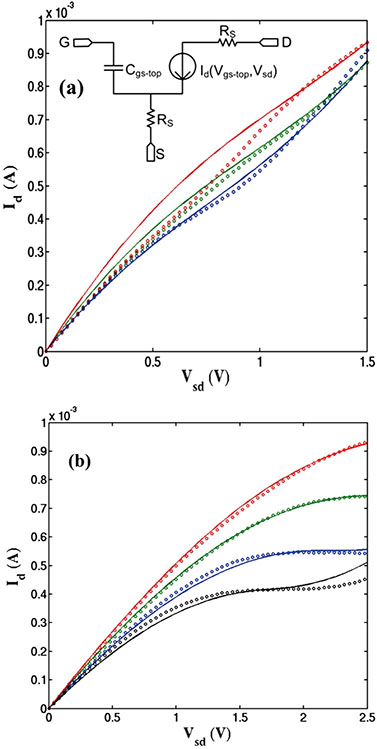
(color online) Current–voltage characteristics of GFET device. Drain current 


