Two-dimensional materials for ultrafast lasers
Wang Fengqiu
       

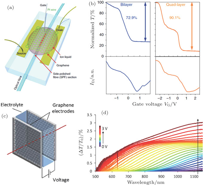
(color online) (a) Schematic diagram of gate-variable all-fibre graphene device. The side-polished fiber (SPF) was fabricated using a standard single-mode optical fiber where two metal electrodes were deposited with 50-nm thickness at both sides of the side-polished region. After transferring the graphene layer, ion liquid was applied to the graphene. Two electrodes and a Pt wire were used as source, drain and gate, respectively.[65] (b) Gate-controlled optical properties of all-fiber devices with bi-(left panels) and quad-layer (right panels) graphene. The bottom panels correspond to electrical transport properties of devices with bi- and quad-layer graphene.[65] (c) Schematic of the voltage-controlled graphene SA based on the supercapacitor structure.[66] (d) Variation of the normalized change of the optical transmission of the graphene as a function of the wavelength at different bias voltages in the 0–3 V range.[66]