† Corresponding author. E-mail:
Using the first-principles calculations, we study the structural, electronic, and magnetic properties of vanadium adsorbed MoSe2 monolayer, and the magnetic couplings between the V adatoms at different adsorption concentrations. The calculations show that the V atom is chemically adsorbed on the MoSe2 monolayer and prefers the location on the top of an Mo atom surrounded by three nearest-neighbor Se atoms. The interatomic electron transfer from the V to the nearestneighbor Se results in the polarized covalent bond with weak covalency, associated with the hybridizations of V with Se and Mo. The V adatom induces local impurity states in the middle of the band gap of pristine MoSe2, and the peak of density of states right below the Fermi energy is associated with the V-dz 2 orbital. A single V adatom induces a magnetic moment of 5 μB that mainly distributes on the V-3d and Mo-4d orbitals. The V adatom is in high-spin state, and its local magnetic moment is associated with the mid-gap impurity states that are mainly from the V-3d orbitals. In addition, the crystal field squashes a part of the V-4s electrons into the V-3d orbitals, which enhances the local magnetic moment. The magnetic ground states at different adsorption concentrations are calculated by generalized gradient approximations (GGA) and GGA+U with enhanced electron localization. In addition, the exchange integrals between the nearest-neighbor V adatoms at different adsorption concentrations are calculated by fitting the first-principle total energies of ferromagnetic (FM) and antiferromagnetic (AFM) states to the Heisenberg model. The calculations with GGA show that there is a transition from ferromagnetic to antiferromagnetic ground state with increasing the distance between the V adatoms. We propose an exchange mechanism based on the on-site exchange on Mo and the hybridization between Mo and V, to explain the strong ferromagnetic coupling at a short distance between the V adatoms. However, the ferromagnetic exchange mechanism is sensitive to both the increased inter-adatom distance at low concentration and the enhanced electron localization by GGA+U, which leads to antiferromagnetic ground state, where the antiferromagnetic superexchange is dominant.
Recently, two-dimensional (2D) materials have received a lot of attention because of their potential applications in a wide range of electronic devices, especially in spintronics. In particular, graphene is considered as the most promising candidate for future electronics.[1] However, pristine graphene is metallic without an energy band gap, which may hinder its direct application in semiconducting devices. Layered transition metal dichalcogenides (LTMDs), such as MoS2, have been discovered to be a new class of 2D materials. Unlike graphene, the LTMDs are semiconducting with a band gap of 1 eV~2 eV, which makes them promising for low-dimensional semiconducting devices. The LTMDs can be readily prepared by micromechanical exfoliation,[2,3] liquid exfoliation,[4,5] hydrothermal synthesis, and chemical vapor deposition.[1,6] Due to the reduction of dimension, the LTMDs exhibit electronic, mechanical, and optical properties different from their three-dimensional (3D) counterparts, and have received a great deal of theoretical[7,8] and experimental attention.[9,10]
Since pristine MoSe2 monolayer is nonmagnetic, many efforts have been devoted to inducing magnetism. Intrinsic defect, strain, and doping or adsorption of foreign atoms have been proposed to be efficient ways to induce magnetism to LTMDs, and the structural, electronic, and magnetic properties can also be tailored, which make LTMDs promising candidates for spintronic devices. These modifications have been much more extensively investigated for MoS2 [11–14] and WS2 [15–18] monolayers than for MoSe2. Investigations on the modifications of MoSe2 monolayer are limited so far. Ghosh et al. found that electronic and optical properties of monolayer MoSe2 can be modulated by equibiaxial strain.[19] Zhang et al. studied the effects of vacancy and strain on the magnetic property of monolayer MoSe2.[20] Ma et al. explored the vacancy-doped and nonmetal adsorbed MoSe2 monolayer.[17]
In the present work, we select MoSe2 monolayer, a two-dimensional (2D) semiconductor with a direct band gap, as the host material, and study its structural, electronic, and magnetic properties with V adatoms at various adsorption concentrations by using first-principles calculations. The electronic structure calculations show that the V adatom is chemically adsorbed on the MoSe2 monolayer, and introduces impurity levels in the middle of the pristine band gap. The magnetic property calculations show that the V adatom induces a magnetic moment in an otherwise nonmagnetic MoSe2 monolayer. Further calculations on the magnetic coupling between the V adatoms show that the magnetic ground state depends on not only the adsorption concentration but also the on-site Coulomb repulsion of the V-3d orbitals. The calculations with generalized gradient approximation (GGA) show a transition from ferromagnetic (FM) to antiferromagnetic (AFM) ground state, while the GGA+U calculations lead to AFM ground state for all investigated concentrations. We propose a ferromagnetic exchange mechanism involving the on-site exchange of Mo and the hybridization between Mo and V, to explain the FM coupling at a short distance between the V adatoms. Both the increased inter-adatom distance at low concentrations and the enhanced electron localization by GGA+U weaken the FM exchange mechanism, and lead to AFM ground state, where the AFM superexchange is dominant and in agreement with the value estimated from the calculated density of states (DOS).
The first-principles calculations are based on density functional theory (DFT), and implemented by the Vienna ab initio simulation package (VASP).[21] The exchange and correlation are treated by the Perdew–Burke–Ernzerhof (PBE) parameterization of GGA.[22] The projector augmented plane-wave (PAW) method is adopted to describe the electron–ion interaction,[23] and the plane-wave cutoff energy is set to be 450 eV. A vacuum layer of 15 Å in thickness is used to isolate the interaction between the MoSe2 sheet and its periodic images along the z-axis. The atomic structures of 2 × 2, 3 × 3, and 4 × 4 supercells are optimized by using conjugate gradient algorithm with a 7 × 7 × 1 Monkhorst–Pack k-mesh for the first two and with a 3 × 3 × 1 k-mesh for the last one, until the residual force on each atom is less than 0.02 eV/Å and the total energy difference between two consecutive ionic steps is less than 10−5 eV. After the structural optimization, the electronic and magnetic properties are calculated with a denser k-mesh of 7 × 7 × 1 and a higher accuracy of total energy of 10−6 eV for all supercells. In addition to the GGA calculations, the electronic structure and magnetic properties are calculated by using GGA+U (GGA plus on-site Coulomb repulsion),[24] where the U parameter is chosen to be 3.0 eV for the V-3d orbitals.[25] The magnetic couplings at different adsorption concentrations are calculated by using both GGA and GGA+U approaches. The valence electron configurations are 4s24p4, 4d55s1, and 3d34s2 for Se, Mo, and V, respectively.
MoSe2 monolayer is comprised of the Se, Mo, and Se atom layers stacked along the z axis, where the Mo layer is sandwiched between two layers of Se. The MoSe2 mono-layer belongs to space group 
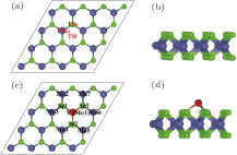
For the V atom adsorbed MoSe2 sheet, three possible high-symmetry positions have been considered as shown in Fig.
 | (1) |
To examine the influence of V adatom on the structure of MoSe2 monolayer, the structural relaxation induced by the V adsorption is measured. Table
| Table 1.
Calculated structure parameters of the MoSe2 monolayer with a V adatom: the stablest adsorption site (site), adsorption energy (E ad), distance between the V adatom and the nearest neighbor Mo atom (d V−M o), distance between the V adatom and the nearest neighbor Se atom (d V−S e), corrugation (C M), adsorption height (h V), and total magnetic moment (M tot). . |
The distortion is attributed to the covalent bond between the V adatom and the three nearest-neighbor Se atoms, associated with the charge transfer from the V to the Se atoms. The charge density difference is illustrated in Fig.
 | (2) |
| Table 2.
Values of local magnetic moment (M) and the charge transfer (Q). The positive (negative) Q values represent accepting (losing) electrons. NN represents the nearest neighbor of the V atom. 2nd NN and 3rd NN represent the second- and third-nearest-neighbor of the V atom. . |
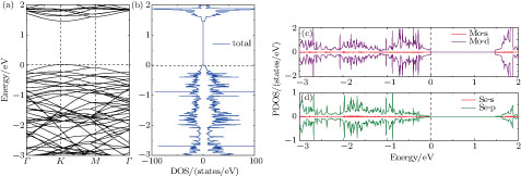
The electronic band structure, and the total and projected density of states (TDOS and PDOS) of the pristine 4 × 4 MoSe2 monolayer are plotted in Fig.
 | Fig. 4. (color online) Electronic band structure (a), total DOS (b), and DOS projected on Mo (c) and Se (d) of pristine 4 × 4 MoSe2 monolayer. The Fermi level is aligned to zero. |
The adsorption of V atom induces magnetism, and the majority and minority spins become asymmetric [Figs.
Integrating the total DOS over the whole energy range results in 149 majority and 144 minority spins. A single V adatom with 5 valence electrons thus induces 5 µB net magnetic moment, approximately equal to that induced for an MoS2 monolayer.[27] The induced magnetic moment is associated with the mid-gap impurity states of majority spin, where two of them (d
xy
and 
The local magnetic moment on the V adatom inside the muffin-tin radius is 3.331 µB, a major contribution to the total magnetic moment. The local magnetic moment on the Mo atom right below the V adatom is 0.377 µB, and that of the six third-nearest neighbor Mo atoms in total is 0.669 µB (Table
In order to observe the detailed distribution of magnetic moment, we depict spin density isosurface in Fig.
 | Fig. 6. (color online) Isosurfaces at spin density 0.001 e/Å3 of V-adsorbed MoSe2 monolayer in top (a) and side (b) views. Yellow and cyan colors represent majority and minority spin densities. |
In addition, compared with the ideal value of 3 µB of a free V atom, the local magnetic moment of V adatom is slightly increased by 0.331 µB, which is attributed to the inter-orbital charge transfer. Compared with that contributed by the free V atom configuration (3d34s2), the magnetic moments contributed by the 4s and 3d orbitals are 0.069 and 3.223 µB for the V adatom.
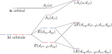
Under the C
3V
local symmetry from the Se trigonal prism, the five 3d orbitals of V adatom will split into a singlet d
z
2
with A1 symmetry, and two doublets (d
xz
, d
yz
) and (
We investigate the magnetic ground state and magnetic coupling between the nearest-neighbor V adatoms. The 2 × 2, 3 × 3, and 4 × 4 supercells are doubled along one edge in the ab plane into 4 ×2, 6×3, and 8×4, respectively, to investigate the influence of adsorption concentration on magnetic ground state.[32,33] The energy differences between the AFM and the FM states, ∆E = E
AFM − E
FM, are calculated and listed in Table
 | (3) |

| Table 3.
Energy differences between the AFM and FM states, ∆E = E
AFM − E
FM, for the V-adsorbed MoSe2 monolayer by GGA and GGA+U approaches at different adsorption concentrations. The d
V−V is the distance between the V atoms, J is the exchange interaction calculated from ∆E, w, and U
eff are the bandwidth of V impurity band and the effective on-site Coulomb repulsion from DOS, J
2 is the AFM superexchange estimated from Eq. ( |
The results calculated with GGA indicate that the sign of the magnetic coupling changes from positive to negative value with increasing V–V distance. When the V–V distance is 6.639 Å, corresponding to an adsorption concentration of 1/12, the magnetic coupling between the two adatoms is FM, and the local magnetizations on the two nearest-neighbor adatoms tend to be parallel to each other. However, when the V–V distance increases to 9.958 Å, the magnetic coupling flips its sign and the magnetic ground state becomes AFM. This result is in qualitative agreement with the results in BN monolayer decorated with foreign atoms[35] and other 2D diluted magnetic systems.[36] However, GGA+U calculations lead to AFM magnetic ground states and couplings at all distances. It also induces a monotonic and faster damping of the magnetic coupling, of which the magnitude decreases from 42.0 meV at 6.639 Å to 0 at 13.278 Å. This is also found in other diluted magnetic insulators, such as V-doped anatase TiO2.[25]
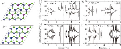
For a better understanding of the magnetic coupling, we calculate the DOSs of the magnetic ground states of the 4 × 2 and 6 × 3 supercells by GGA and GGA+U [Figs.
In fact, a strong FM exchange mechanism in the 4 × 2 supercell by GGA is associated with the Mo atom shared by two nearest-neighbor V adatoms as a 3rd nearest neighbor. From the isosurface of spin density (Fig.
The strength of the above FM exchange can be estimated on the assumption that the on-site exchange energy follows the Dudarev formulation,
 | (4) |
 | (5) |
Since two nearest-neighbor V adatoms share a 3rd nearestneighbor Mo atom and each V adatom has 6 nearest neighbors in the lattice shown in Fig.
 | (6) |
Using the typical value of on-site exchange for 4d atoms, I ~ 0.2 eV, and the total magnetic moment on Mo given by Table
It is obvious that the above FM exchange mechanism is sensitive to both inter-adatom distance and on-site Coulomb repulsion. When the inter-adatom distance is increased, two nearest-neighbor V adatoms will no longer share a 3rd nearestneighbor Mo atom, and thus the FM exchange mechanism will vanish. When extra on-site Coulomb repulsion is applied to V-d orbitals by GGA+U approach, the enhanced on-site Coulomb repulsion will significantly reduce the Mo–V hybridization and thus the total magnetic moment is shared by Mo atoms, which results in a much smaller ∆E ' .
When the inter-adatom distance increases or extra on-site Coulomb repulsion is applied, the dominant exchange mechanism will be the AFM superexchange,[42]
 | (7) |
In this study, we carry out the first-principles calculations to investigate the structural, electronic, and magnetic characteristics of V-adsorbed MoSe2 monolayer. The calculations indicate that the most favorable adsorption site is on the top of a Mo atom, and that the V adatom can induce impurity states in the middle of the band gap, which are mainly from the V-3d states with hybridization of the Mo-4d and Se-4p states. The V adatom induces magnetism for the MoSe2 monolayer, which is associated with the mid-gap impurity states of majority spin. Further, the inter-orbit electron transfer from V-s to V-d slightly enhances the local magnetic moment on the V adatom. The magnetic ground state depends on not only the adsorption concentration but also the on-site Coulomb repulsion. A ferromagnetic exchange mechanism is proposed to explain the FM ground state given by GGA calculations at a high adsorption concentration of 1/12, based on the on-site exchange of Mo and the hybridization between Mo and V. The AFM superexchanges are also estimated by using the parameters extracted from the calculated DOS.
| [1] | |
| [2] | |
| [3] | |
| [4] | |
| [5] | |
| [6] | |
| [7] | |
| [8] | |
| [9] | |
| [10] | |
| [11] | |
| [12] | |
| [13] | |
| [14] | |
| [15] | |
| [16] | |
| [17] | |
| [18] | |
| [19] | |
| [20] | |
| [21] | |
| [22] | |
| [23] | |
| [24] | |
| [25] | |
| [26] | |
| [27] | |
| [28] | |
| [29] | |
| [30] | |
| [31] | |
| [32] | |
| [33] | |
| [34] | |
| [35] | |
| [36] | |
| [37] | |
| [38] | |
| [39] | |
| [40] | |
| [41] | |
| [42] |


