Theoretical investigation of hierarchical sub-wavelength photonic structures fabricated using high-order waveguide-mode interference lithograph
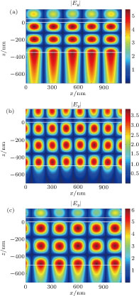
(color online) Simulated electric field |E y| of TE2-mode interference in multilayer film. The white lines indicate the interfaces of glass, Ag, photoresist, and air, from top to bottom. (a) Values of the prism and photoresist RI are 1.7 and 1.8, respectively; the photoresist thickness is 345 nm. (b) The values of RI for prism and photoresist are the same as in (a); the photoresist thickness is 500 nm. (c) The values of the prism and photoresist RI are 1.7 and 1.5, respectively, and the photoresist thickness is 500 nm.