Electrical and dielectric properties of Na1/2La1/2Cu3Ti4O12 ceramics prepared by high energy ball-milling and conventional sintering
Mahfoz Kotb H1, 2, †, , Ahmad Mohamad M1, 3, ‡,
Department of Physics, College of Science, King Faisal University, Al-Hassa 31982, Saudi Arabia
Department of Physics, Faculty of Science, Assiut University, Assiut 71516, Egypt
Department of Physics, Faculty of Science, Assiut University, The New Valley, El-Kharga 72511, Egypt


† Corresponding author. E-mail: hkotb@kfu.edu.sa

‡ Corresponding author. E-mail: mmohamad@kfu.edu.sa

Abstract
Abstract

We report on the measurements of the electrical and dielectric properties of Na1/2La1/2Cu3Ti4O12 (NLCTO) ceramics prepared by high energy ball-milling and conventional sintering without any calcination steps. The x-ray powder diffraction analysis shows that pure perovskite-like CCTO phase is obtained after sintering at 1025 °C–1075 °C. Higher sintering temperatures result in multi-phase ceramics due to thermal decomposition. Scanning electron microscope observations reveal that the grain size is in a range of ∼3 μm–5μm for these ceramics. Impedance spectroscopy measurements performed in a wide frequency range (1 Hz–10 MHz) and at various temperatures (120 K–470 K) are used to study the dielectric and electrical properties of NLCTO ceramics. A good compromise between high ε′ (5.7 × 10³ and 4.1 × 10³ at 1.1 kHz and 96 kHz, respectively) and low tan δ (0.161 and 0.126 at 1.1 kHz and 96 kHz, respectively) is obtained for the ceramic sintered at 1050 °C. The observed high dielectric constant behavior is explained in terms of the internal barrier layer capacitance effect.

1. Introduction

Since 2000, the giant dielectric constant (GDC) materials (ε′ > 103) have been extensively studied.[151] This is because of their potential applications in various electronic fields such as the charge storage capacitors.[9,10] These studies have resulted in the discovery of a large variety of GDC materials, mostly perovskite oxides, i.e., CuO,[11,12] [AC3](B4)O12 (where A = Ca, Cd, Sr, Na or Th; B = Ti; and C = Cu2+ or Mn3+),[1,1319,29] (M, N)-doped NiO (where M = Li, Na, K, and N = Ti, Al, Si, Ta),[20,21] A(Fe1/2B1/2)O3 (where A = Ba, Sr, Ca and B = Nb, Ta, Sb),[22,23] and BaTi1–x(Ni1/2W1/2)xO3.[24] Nevertheless, CaCu3Ti4O12 (CCTO) is still the most studied material because of its special properties: room temperature dielectric constant value, ε′ of ∼ 103–104 that is independent of temperature and frequency over a wide range. Unfortunately, the loss tangent, tan δ of CCTO ceramics is still too large (> 0.05) which is an obstacle toward the application of CCTO to capacitor. Some new CCTO-related oxide ceramics are nowadays attracting the attention due to their low dielectric losses.[2527] Low values of tan δ of 0.030–0.041 (1 kHz) and 0.022 (1 kHz) were reported for Na0.5Sm0.5Cu3Ti4O12[28] and La-doped Na0.5Bi0.5Cu3Ti4O12,[29] respectively. These results indicate that Na0.5Ln0.5Cu3Ti4O12 (Ln = La, Sm, Gd, Dy, Yb, and Y) ceramics may have a potential application to capacitor. Thongbai et al.[30] prepared Na0.5La0.5Cu3Ti4O12 by solid state reaction method in a process including two calcination steps (at 950 °C for 15 h and at 1000 °C for 10 h) followed by 5 h sintering at 1080 °C–1090 °C. The final ceramics showed an average grain size of 4 μm, ε′ ∼ 6.1–8.7 × 10³ and tan δ ∼ 0.032–0.038 at 10 kHz. Liu et al.[31] prepared Na0.5La0.5Cu3Ti4O12 by sol–gel method including a sintering step at 1060 °C–1100 °C for 5 h–15 h. The ceramics sintered at 1080 °C for 10 h exhibited homogeneous microstructure with an average grain size of about 4 μm, ε′ of 1.1 × 10⁴–1.8 × 10⁴ and tan δ of 0.051–0.064 at 1 kHz–10 kHz which are about twice higher than the dielectric constant and loss tangent values reported by Thongbai et al.[30] This variation in the reported values of ε′ and tan δ for the same material reflects the dependence of the ceramics’ properties on the preparation method. In fact, the preparation method controls the microstructure, particularly the grain size and the electrical conductivity of the grain and grain boundaries which are determinant parameters for the dielectric properties of the GDC ceramics.[16,32,33]

In the present study we have prepared NLCTO by a simplified solid state reaction where the calcination step is dismissed. The powder of NLCTO is synthesized by high-energy ball milling technique. The dense and pure phase ceramics are obtained by conventional furnace sintering method. The influences of sintering temperature on the structural and dielectric properties of the prepared ceramics are also studied.

2. Experiment

In this work, Na1/2La1/2Cu3Ti4O12 (NLCTO) powder was synthesized by mechanochemical milling of stoichiometric amounts of high-purity La2O3 (99.99%), TiO2 (99.9%), CuO (99.99%), and Na2CO3 (99.99%) in 2-propanol medium. The milling process was carried out by using Fritsch P-7 premium line machine for 30 h with a rotation speed of 500 rpm using a 45-ml tungsten carbide pot and tungsten carbide balls where the ball-to-powder mass ratio was 8:1. The resulting powder was then pressed into pellets each with 12 mm in diameter and 2 mm in thickness. Dense ceramics were obtained by sintering the pellets in air at 1025 °C, 1050 °C, 1075 °C, and 1100 °C for 10 h with a heating rate of 4 °C/min. The ceramics sintered at these temperatures are referred to as NLCTO-25, NLCTO-50, NLCTO-75, and NLCTO-00, respectively. The densities of the sintered pellets were calculated from their dimensions and weights. The prepared ceramic materials were characterized by field emission scanning electron microscope (FE-SEM) (Joel, SM7600F) technique. The x-ray diffraction (XRD) data were collected over the 0° ≤ 2θ ≤ 90° range using a Stoe Stadi-P Image Plate, IP, (Stoe and Cie GmbH, Darmstadt,Germany), with monochromated Cu Kα 1 radiation (λ = 1.5406 Å). The prepared ceramics have been crushed and ground into fine powder in an agate mortar before XRD measurements. Impedance spectroscopy (IS) measurements were performed by turnkey concept 50 system from Novocontrol over the 1 Hz–40 MHz frequency range. IS measurements were performed in dry nitrogen atmosphere in a 120 K–500 K temperature range, where the temperature was controlled by the Quatro Cryosystem. Silver paint was used as electrodes.

3. Results and discussion

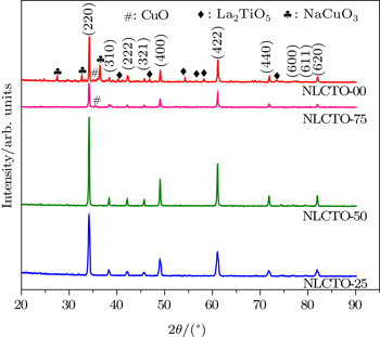
Figure 1 shows the XRD patterns of the prepared NLCTO ceramics (NLCTO-25, NLCTO-50, NLCTO-75, and NLCTO-00). The main diffraction peaks in these patterns could be indexed to a body-centered cubic perovskite-related structure of space group Im3 according to JCPDS card # 75-2188 of CCTO. The lattice parameters were calculated to be 7.428, 7.424, 7.423, and 7.412 Å for the ceramics NLCTO-25, NLCTO-50, NLCTO-75, and NLCTO-00, respectively. These values are in accordance with those reported in Refs. [30] and [34]. It is noticed from Fig. 1 that the diffraction peaks of NLCTO-50 are comparatively more intense, which indicates better crystallinity or less defects of this ceramic than those of the other ceramics. No secondary phases are detected in NLCTO-25 and NLCTO-50 ceramics while a CuO impurity phase is observed in NLCTO-75. The ceramic composition of NLCTO-00 is found to be composed of CCTO phase with some other secondary phases which might be due to thermal decomposition of NLCTO at this temperature. It is likely that decomposition of Cu or Na is the major cause for this observation as observed in Na1/2Sm1/2Cu3Ti4O12[28] and CCTO[35] ceramics. The secondary phases in NLCTO-00 could be identified as the CuO (JCPDS No: 03-0884), NaCuO2 (JCPDS No: 85-2391), and La2TiO5 (JCPDS No: 75-2394). Considering these findings, only NLCTO-25, NLCTO-50, and NLCTO-75 will be electrically investigated as it is composed of nearly pure CCTO phase.

Fig. 1. XRD patterns of the NLCTO ceramics.

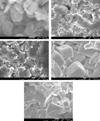
Figure 2 reveals the SEM images of the nano-powder of NLCTO prepared by mechanical milling and the fractured surface of the current NLCTO ceramics. According to Fig. 2(a), the crystallite size for the powder is ∼ 30 nm. All the present ceramics have shown the grain–grain boundary structures. With increasing sintering temperature, the grain sizes increase from ∼ 3 μm–5 μm for the ceramics NLCTO-25, NLCTO-50, and NLCTO-75 to ∼ 30 μm for NLCTO-00. The densities of the prepared pellets are measured to be 4.54, 4.63, and 4.69 g/cm3 for NLCTO-25, NLCTO-50, and NLCTO-75, respectively.

Fig. 2. FE-SEM morphologies of (a) the NLCTO powder and the fractured surface of NLCTO ceramics, (b) NLCTO-25, (c) NLCTO-50, (d) NLCTO-75, and (e) NLCTO-00.

Figure 3(a) shows the EDX spectra of the grain-boundary regions for NLCTO-50 as a representative example. Table 1 summarizes quantitatively the EDX results for the current ceramics. All the constituent elements could be detected in the grain and grain boundaries. Though the grains for all the studied ceramics were nearly stoichiometric, the grain boundaries of NLCTO-50 were comparatively rich in La and Cu.

Figure 3(b) shows the Cu mapping by EDX of the surface of NLCTO-75. It can be seen that at a sintering temperature of 1075 °C, Cu tends to migrate toward the intergranular region. This should be the CuO secondary phase detected in Fig. 1 for NLCTO-75.

Table 1.

Elemental analyses of the grain and grain boundary regions for NLCTO ceramics.

.
Fig. 3. (a) EDX spectrum of the grain boundary for NLCTO-50 and (b) the EDX mapping of Cu from the surface of the NLCTO-75.

Figure 4 reveals the variations in ε′ and tan δ at selected temperatures for NLCTO-25, NLCTO-50, and NLCTO-75. All the ceramics exhibit high dielectric constant (ε′ > 103) over a wide range of frequencies (1 Hz–106 Hz), which drops down to ε′ ∼ 100 at frequencies higher than 106 Hz with the dropping frequency increasing with temperature rising. This relaxation in ε′ is accompanied by a loss peak of tan δ which shifts toward higher frequencies with increasing temperature as seen in Figs. 4(a)4(c). The same behavior has been previously reported for CCTO and its related materials.[7,31] Besides, the increase in ε′ which is associated with a strong increase in tan δ for all ceramics at low frequencies and high temperatures is believed to be due to the increase of electrical conductivity and/or electrode polarization effects.[36,37]

The values of ε′ and tan δ at selected temperatures and frequencies for the studied NLCTO ceramics are given in Table 2. From these findings, it is clear that the dielectric properties of NLCTO-50 represent a good compromise among the high ε′ (5.7 × 10³ and 4.1 × 10³ at 1.1 kHz and 96 kHz, respectively), frequency stability of ε′ and low tan δ (0.161 and 0.126 at 1.1 kHz and 96 kHz, respectively). The better dielectric properties of NLCTO-50 should be closely correlated with the observed Cu-rich grain boundaries in these samples. The occurrence of Cu-rich phase in the grain boundaries and its role in enhancing the dielectric properties have been previously reported for Y2/3Cu3Ti4O12[38] and CCTO.[39] Even if a direct comparison with literature is difficult due to the different preparation methods and conditions used, we argue that the results in the present work are comparable to those reported in the literature: ε′∼ 8.7 × 10³ & tan δ ∼ 0.114 (at 1.1 kHz) for NLCTO ceramics prepared by conventional solid state reaction[30] and ε′∼ 1.53 × 10⁴ & tan δ ∼ 0.063 at 1 kHz for NLCTO ceramics prepared by sol–gel method.[31]

Table 2.

Values of ε′ and tan δ, measured at 310 K for NLCTO ceramics.

.

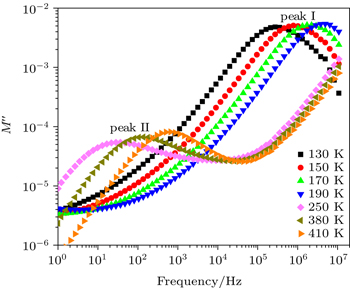
For more understanding of the dielectric relaxation in the current ceramics, we use the frequency dependence of the imaginary part of the electrical modulus M″ plots since this formalism identifies only the electrical responses with small capacitances. Thus, in the M″ spectra the electrode effects are usually suppressed. Figure 5 depicts the M″ spectra for the NLCTO-25 ceramics at different temperatures as a representative example. As can be seen from Fig. 5, there are two relaxation peaks: peak I which starts to appear at lower temperature and high frequency. The second peak, peak II, appears at temperature higher than room temperature and low frequency. Since the M″ peak maximum is inversely proportional to the capacitance of the element responsible for the peak,[40] then peak I and peak II are attributed to the electrical responses of the grain and grain boundary elements, respectively. For both responses, the corresponding M″ peaks shift toward higher frequencies with increasing temperature, which indicates thermally activated mechanism.
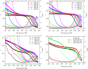
Fig. 4. Frequency dependences of ε′ and tan δ for (a) NLCTO-25, (b) NLCTO-50, (c) NLCTO-75 at selected temperatures, and (d) all NLCTO ceramics at 300 K.
Fig. 5. Frequency dependences of the imaginary part of electric modulus, M″ for NLCTO-50 at different temperatures.

Since the frequency of M″ peak (fmax) is related to the mean value of the relaxation time (τ) as τ = 1/2π fmax, τ could be calculated at different temperatures. It has been found that the temperature dependence of the calculated values of τ follows the Arrhenius law:

where τ0 is the pre-exponential factor, ER is the activation energy for the relaxation process, and kB is the Boltzmann constant. The data fitted to Eq. (1) are shown in Fig. 6. The calculated values for the activation energy of relaxation in grain (ER.g) and grain boundary (ER.g.b) of the present ceramics are given in Table 3. The ER.g. values for the NLCTO-25, NLCTO-50, and NLCTO-75 ceramics are all ∼ 0.10 eV which is comparable to those reported in literature of CCTO ceramics family. Nevertheless, ER.g.b. values are found to decrease considerably with increasing the sintering temperature. ER.g.b. values for NLCTO-25, NLCTO-50, and NLCTO-75 ceramics are 0.745 eV, 0.677 eV, and 0.268 eV, respectively. These values of ER.g.b. for the present NLCTO ceramics are in the ranges of 0.1 eV–0.5 eV and 0.6 eV–1.2 eV for the activation energies for the single-ionized and doubly-ionized oxygen vacancies, respectively.[41] Oxygen vacancies in oxide ceramics are produced during the high-temperature sintering step.[4,42]

Table 3.

Activation energy values, in unit eV, for conduction (ΔE) and for relaxation process (ER), and resistivity of grain (Rg) and grain boundary (Rg.b.) for NLCTO ceramics.

.

Giant dielectric values of CCTO ceramics are widely interpreted within the “brick work” model[43] which assumes the ceramic to be composed of semiconducting grains separated by insulating grain boundaries. Considering this model, the polarization effect at insulating grain boundary between semiconducting grains or other internal barriers is the main source for the giant value of dielectric constant. Therefore, it is important to study the electrical properties of the grain boundary and grain interior of the investigated ceramic. For this purpose, impedance spectroscopy was used to characterize and separate its electrical response. Figure 7 shows the impedance complex (Z′–Z″) plane plots, at room temperature, for the ceramics NLCTO-25, NLCTO-50, and NLCTO-75. All the ceramics exhibit a small semicircular arc at high frequency and a large semicircular arc at low frequency. These data are described properly with an equivalent circuit consisting of two parallel RC elements in series[44] as shown in the inset of Fig. 7. Each RC element represents one of the electrical elements of the material. The resistance R of each element can generally be determined from the diameter of the corresponding semicircular arc. It is evident from Fig. 7 that the present ceramics are electrically inhomogeneous where each ceramic is composed of highly resistive element and a semiconductive one which is in accordance with the “brick work” model.

Fig. 6. Plots of logrithmic relaxation time τ versus 1000/T for NLCTO ceramics. Solid and empty symbols refer to the grains and grain boundaries, respectively.

According to this model, the higher frequency semicircular arc of the impedance corresponds to the response of the grains, while the semicircular arc at low frequency corresponds to the response of the grain boundaries.[13] It is worth noting in the case that only a low-frequency semicircular arc exists, the resistivity of the grains can be determined from the non-zero intercept at the high-frequency limit.[45,46]

Figure 8 shows the impedance complex plane plots at selected temperatures for NLCTO-50, as a representative example. It can be seen from this figure that the resistivities of both grains and grain boundaries decrease with increasing the measurement temperature. Due to the incompleteness of the semicircular arc at low frequency, the grain boundary resistivity is calculated from the (−Z″)–f curve.

Fig. 7. Room temperature complex impedance spectra of NLCTO ceramics.
Fig. 8. Impedance complex plane for the NLCTO-50 ceramic at different temperatures.

The frequency dependences of (−Z″) at selected temperatures for NLCTO-50 are given in Fig. 9. All the ceramics show the same behaviours where the value of the peak-maximum decreases and its position shifts towards higher frequency with increasing temperature. Considering the brick-work model, (−Z″) is related to the angular frequency (ω) by

Therefore, for the electrically inhomogeneous material with RgRg.b. it can be easily proven that the peak-maximum value of −Z″ (ω) is related to the resistivity of grain boundary by

The determined values of grain and grain boundaries resistivities Rg and Rg.b. at 310 K for the current ceramics are given in Table 3. It is observed that the grain resistivity is less sensitive to the sintering temperature in contrast to the grain boundaries behaviour. NLCTO-50 has the lowest grain resistivity value (151 Ω·cm) which might be due to the better crystallinity of NLCTO-50 as approved by XRD measurements (Fig. 1). Moreover, the grain-boundary resistivity is found to differ by four orders of magnitude with sintering temperature increasing from 1025 °C to 1075 °C.

Fig. 9. Frequency dependences of Z″ for the NLCTO-50 ceramic at different temperatures.

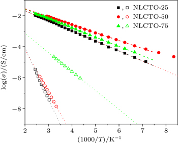
Figure 10 reveals the temperature dependences of the electrical conductivity (σ = 1/ρ) of grain and grain boundary for NLCTO ceramics. According to this figure, the variation of the conductivity with temperature obeys the Arrhenius relation:

where σ0 is the pre-exponential factor and ΔE is the activation. The calculated values of the activation energy of the conduction in the grain, ΔEg, and grain boundary, ΔEg.b., for the investigated ceramics are summarized in Table 3.

The obtained values of ΔEg (∼ 0.10 eV–0.129 eV) for the conduction in the grains in the present NLCTO ceramics are in good agreement with the values of ΔEg in the literature for CCTO and its related materials.[4749] Nevertheless, ΔEg.b. is found to decrease considerably from 0.658 eV to 0.243 eV with sintering temperature increasing from 1025 °C to 1075 °C. The values of ΔEg.b. for the NLCTO-25 and NLCTO-50 lie in a range of 0.5 eV–0.7 eV that is widely found in the literature for CCTO-related materials.[4547] It is worth noting that the value of ΔEg.b. for the NLCTO-75 is similar to the reported values of Bi2/3Cu3Ti4O12[50] and La3+ and Nb5+ co-doped CCTO[51] ceramics. The low value of ΔEg.b. for NLCTO-75 is likely to be related to the existence of intergranular CuO phase which has been approved by XRD and EDX analysis as discussed above. This result suggests the partial replacement of Cu2+ by La3+ in the grain boundaries, resulting in the increase of the grain boundary conductivity due to the higher density of free electrons. It is noticed from Table 3 that the values of the activation energy for conduction (ΔE) are very close to those of the activation energy for relaxation (ER). Besides, both ΔE and ER vary in the same manner with increasing sintering temperature. These results may suggest that the conduction and the relaxation processes in the present ceramics have the same origin.

Fig. 10. Arrhenius plots of grain and grain boundary conductivity for NLCTO ceramics. Solid and empty symbols represent the grains and grain boundaries, respectively.
4. Conclusions

Na1/2La1/2Cu3Ti4O12 (NLCTO) ceramics are successfully prepared by high-energy ball-milling and conventional sintering without any calcination steps. The phase formation analysis reveals that the ceramics sintered at 1025 °C–1075 °C consist of pure CCTO-like crystallographic structures. Sintering at 1100 °C results in thermal decomposition and subsequently the formation of a ceramic with multiphase structure. The present NLCTO ceramics have high values of ε′ in a range of ∼ 3.8 × 10³–9.6 × 10³ and 2.3 × 10³–4.1 × 10³ at 1.1 kHz and 96 kHz, respectively and tan δ of ∼ 0.161–2.075 and 0.126–0.440 at 1.1 kHz and 96 kHz, respectively. Complex impedance and complex electric modulus analysis reveal the electrically heterogeneous structure of the present NLCTO ceramic. Thus, the observed high dielectric constant behavior is explained in terms of the internal barrier layer capacitance effects.

Reference
1Subramanian M ALi DDuan NReisner B ASleight A W 2000 J. Solid State Chem. 151 323
2Ren HLiang PYang Z 2010 Mater. Res. Bull. 45 1608
3Brunet MMafhoz Kotb HBouscayrol LScheid EAndrieux MLegros CSchamm-Chardon C 2011 Thin Solid Films 519 5638
4Kim C HJang Y HSeo S JSong C HSon J YYang Y SCho J H 2012 Phys. Rev. 85 245210
5Yang ZZhang YLu Z HZhang KXiong RShi J 2013 J. Am. Ceram. Soc. 96 806
6Liang P FChao X LWang FLiu Z QYang Z P 2013 J. Am. Ceram. Soc. 96 3883
7Ahmad M MYamane YYamada K 2013 Mater. Sci. Eng. 178 965
8Liang PChao XYang Z 2014 J. Appl. Phys. 116 044101
9Homes C CVogt TShapiro S MWakimoto SRamirez A P 2001 Science 293 673
10Krohns SLunkenheimer PMeissner SReller AGleich BRathgeber AGaugler TBuhl H USinclair D CLoidl A 2011 Nat. Mater. 10 899
11Chen J WNarsinga R G 2011 IEEE T. Magn. 47 3772
12Deepthi K RPandiyarajan TKarthikeyan B 2013 J. Mater. Sci.: Mater. Electron. 24 1045
13Sinclair D CAdams T BMorrison F DWest A R 2002 Appl. Phys. Lett. 80 2153
14Liu JDuan C GMei W NSmith R WHardy J R 2005 J. Appl. Phys. 98 093703
15Adams T BSinclair D CWest A R 2006 Phys. Rev. 73 094124
16Marchin LGuillemet-Fritsch SDurand BLevchenko A ANavrotsky ALebey T 2008 J. Am. Ceram. Soc. 91 485
17Masingboon CThongbai PMaensiri SYamwong T 2009 Appl. Phys. 96 595
18Hao WZhang JTan YSu W 2009 J. Am. Ceram. Soc. 92 2937
19Ahmad M M 2013 Appl. Phys. Lett. 102 232908
20Jana P KMukherjee SChaudhuri B K 2014 J. Phys. D: Appl. Phys. 47 365302
21Khemprasit JKhumpaitool B 2015 Ceram. Int. 41 663
22Bochenek DNiemiec PAdamczyk M 2015 Eur. Phys. 88 278
23Wang ZLi H JZhang L LWen Y FPu Y P 2015 J. Mater. Sci.: Mater. Electron. 26 134
24Zhao FYue ZPei JZhuang HGui ZLi L 2007 J. Am. Ceram. Soc. 90 2461
25Boonlakhorn JKidkhunthod PThongbai P 2015 J. Eur. Ceram. Soc. 35 3521
26Kum-onsa PThongbai PPutasaeng BYamwong TMaensiri S 2015 J. Eur. Ceram. Soc. 35 1441
27Li JWu KJia RHou LGao LLi S 2016 Mater. & Design 92 546
28Somphan WThongbai PYamwong TMaensiri S 2013 Mater. Res. Bull. 48 4087
29Yang Z PRen H MChao X LLiang P F 2012 Mater. Res. Bull. 47 1273
30Thongbai PYamwong TMaensiri S 2012 Res. Bull. 47 432
31Liu ZJiao GChao XYang Z 2014 J. Mater. Sci.: Mater. Electron. 25 2096
32Shao S FZhang J LZheng PZhong W LWang C L 2006 J. Appl. Phys. 99 084106
33Fang T TMei L THo H F 2006 Acta Mater. 54 2867
34Liang K CLiu H LYang H DMei W NLing D C 2008 J. Phys.: Condens. Matter 20 275238
35Yuan W 2009 J. Phys. D: Appl. Phys. 42 175401
36Meeporn KYamwong TPinitsoontorn SAmornkitbamrung VThongbai P 2014 Ceram. Int. 40 15897
37Wu JNan C WLin YDeng Y 2002 Phys. Rev. Lett. 89 217601
38Liang PLi FChao XYang Z 2015 Ceram. Int. 41 11314
39Ahmad M MAl-Libidi EAl-Jaafari ASyed Ghazanfar SYamada K 2014 Appl. Phys. 116 1299
40Li MFeteria ASinclair D C 2009 J. Appl. Phys. 105 114109
41Liang PLi YZhao YWei LYang Z 2013 J. Appl. Phys. 113 224102
42Wang CZhang M NXu K BWang G J 2012 J. Appl. Phys. 112 034109
43Irvine J T SSinclair D CWest A R 1990 Adv. Mater. 2 132
44Yuan W XLi Z J 2012 J. Phys. Chem. Solids 73 599
45Somphan WSangwong NYamwong TThongbai P 2012 J. Mater. Sci.: Mater. Electron. 23 1229
46Jia RZhao XLia JTa X 2014 Mater. Sci. Eng. 185 79
47Liang PYang ZChao X 2016 J. Alloys. Compd. 678 273
48Ni LChen X M 2010 J. Am. Ceram. Soc. 93 184
49Ahmad M MMahfoz Kotb H 2015 J. Mater. Sci.: Mater. Electron. 26 8939
50Yang LHuang GWang THao HTian Y 2016 Ceram. Int. 42 9935
51Thomas HAbraham KThomas JSaban K V 2015 Ceram. Int. 41 10250