Crosstalk analysis of silicon-on-insulator nanowire-arrayed waveguide grating
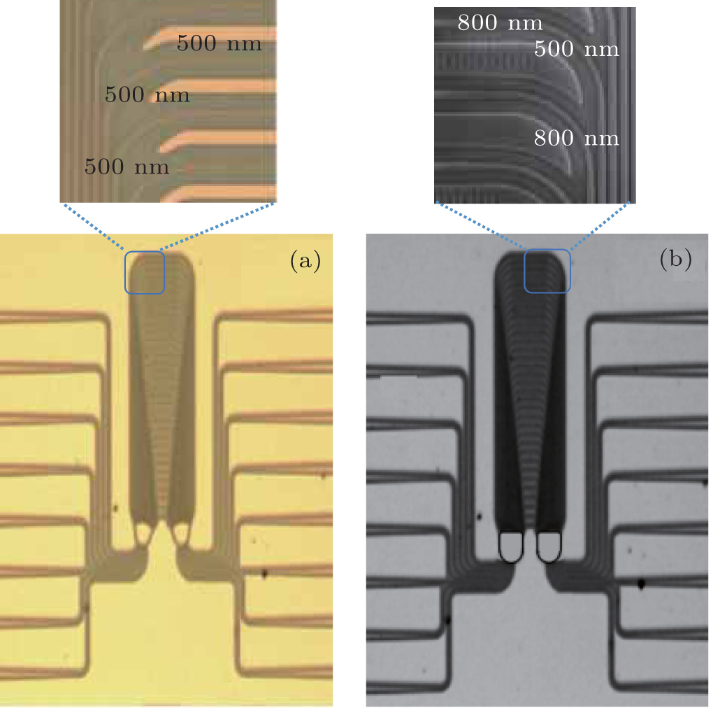
Microscope pictures of SOI nanowire (a) AWG (#1) and (b) AWG (#2). Insets: the detail views of the bends in the arrayed waveguide.

Crosstalk analysis of silicon-on-insulator nanowire-arrayed waveguide grating |
Microscope pictures of SOI nanowire (a) AWG (#1) and (b) AWG (#2). Insets: the detail views of the bends in the arrayed waveguide. |
 |