Lattice structures and electronic properties of WZ-CuInS
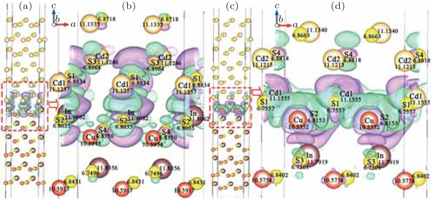
The general Charge density difference (a) and partial enlarged view (b) (including Bader charges) for model A interface; the general charge density difference (c), and partial enlarged view (d) (including Bader charges) for model B interface.

