Analytical threshold voltage model for strained silicon GAA-TFET
Kang Hai-Yan†, , Hu Hui-Yong, Wang Bin
Key Laboratory for Wide Band-Gap Semiconductor Materials and Devices, School of Microelectronics, Xidian University, Xi’an 710071, China


† Corresponding author. E-mail: Kanghaiyan5200@163.com

Project supported by the National Natural Science Foundation of China (Grant No. 61474085).

Abstract
Abstract

Tunnel field effect transistors (TFETs) are promising devices for low power applications. An analytical threshold voltage model, based on the channel surface potential and electric field obtained by solving the 2D Poisson’s equation, for strained silicon gate all around TFETs is proposed. The variation of the threshold voltage with device parameters, such as the strain (Ge mole fraction x), gate oxide thickness, gate oxide permittivity, and channel length has also been investigated. The threshold voltage model is extracted using the peak transconductance method and is verified by good agreement with the results obtained from the TCAD simulation.

1. Introduction

Continuous scaling of traditional metal-oxide-sem-icon-ductor field-effect transistors (MOSFETs) for high performance can result in a rapid increase of power, which blocks its applications in the low power domains.[13] Therefore, tunnel field effect transistors (TFETs) have been considered as one of the most promising candidates for MOSFETs beyond 45 nm for future ultra-low power applications due to their better immunity to short channel effects, higher ION/IOFF ratio, and so on.[47] However, TFETs to date show a low drain current due to the low band-to-band tunneling (BTBT) efficiency.

To boost the tunneling currents, the biaxial strained silicon technology, which reduces the effective carrier transport mass (m*) by lowering and splitting the band gap resulting from the exerted strain in the silicon layer, seems to be an effective way to enhance the tunnel efficiency.[810] Gate all around TFETs (GAA TFETs) with strained silicon can provide enhanced electrostatic performance and optimum scaling capability to improve the current. The gate threshold voltage is a key electrical parameter for designing the TFET. Additionally, to estimate the device current we must know the threshold voltage.[11,12] Although plenty of efforts have been made for the extraction of TFET threshold voltages and some models have been developed, reports on the models for strained silicon TFETs with a GAA architecture have been rare.

In this paper, an analytical threshold voltage model for strained silicon GAA TFETs is developed. Moreover, the effect of the device parameters like the strain (Ge mole fraction x), gate oxide thickness, gate oxide permittivity, and channel length on the threshold voltage have been discussed, which can provide an effective reference for designing the GAA TFET. The model threshold voltage is extracted using peak transconductance method and is in excellent agreement with the TCAD simulation results, giving the evidence for its validity.

2. Structure and analytical model
2.1. Structure of the strained silicon GAA TFET

Figure 1 shows a cross-sectional diagram of a GAA TFET. The proposed cylindrical TFET is constructed mainly by a PIN and surrounding gate, which provides better electrostatic control over the channel. The doping concentrations of the source and drain regions are Ns and Nd, respectively. The intermediate channel is moderately n-doped, with a doping concentration Nc. Lg is the length of the gate, R is the radius of the channel, and Tox is the thickness of the gate oxide layer. Because of the strain (Ge mole fraction x) in Si1−xGex, the energy band gap of the strained silicon GAA TFET changes with the Ge mole fraction x, which is shown in Fig. 2 for x = 0.1 and x = 0.3. As the energy band gap narrows, the tunneling probability increases, and the drain current of a GAA TFET in the ON state improves.

Fig. 1. Cross-sectional diagram of the n-TFET.
Fig. 2. Energy band of the strained-silicon.

GAA TFET is basically a reverse biased PIN diode with the working principle of a quantum mechanical BTBT mechanism.[13] When a positive voltage is applied to the end of the gate and drain over the threshold voltage, the energy band at the source-channel junction is strongly bended, and valence and conduction band overlap occurs, as shown in Fig. 2. Simultaneously, the BTBT current occurs in the GAA TFET. Therefore, the threshold voltage is a key point in the analysis of the current.

2.2. Analytical threshold voltage model

To predict the channel surface potential characteristic of the GAA TFET in the subthreshold region, we assume that the mobile charges in this region are negligible and that source-channel and drain-channel junctions are abrupt. Therefore, the 2D Poisson’s equation at the n-type strained silicon cylindrical channel can be written as

where ϕ(r,z) is the electrostatic potential in the channel region, εssi is the strained silicon region dielectric permittivity, and r varies from zero to R.

To obtain the solution of Eq. (1), a parabolic approximation of the channel potential distribution in the radial direction is applied, which can be written as[14]

The coefficients a0(z), a1(z), and a2 (z) are functions of z only, which can be determined by using the following boundary conditions:

At the interface between the gate oxide and the strained silicon, we assume an electrostatic potential as a surface potential,

At the central axis of the cylinder channel, the electric field is zero,

At the interface between the gate oxide and the strained silicon, the electric field is continuous

Applying the boundary conditions from Eqs. (3)–(5) to Eq. (2), the coefficients can be obtained, and the solution of Eq. (2) can be expressed as

The electric field distribution along the r radius direction can be written as

where is the capacitance of the gate oxide because the gate is all around the oxide. The capacitance can be modified into , Vgs is the voltage across the gate and the source, ϕs(z) is the surface potential of the interface between the gate and the oxide. εox is the permittivity of the gate oxide. Because of the strain, (VFB)ssi is given by

where (VFB)si = ϕMϕsi,

where (VFB)ssi and (VFB)si are the flat-band voltages of the strained silicon and silicon, respectively. ϕM is the metal gate work function. ϕsi and ϕF are the work function and Fermi energy of the silicon, respectively. VT = kT/q is the thermal voltage, and nissi is the intrinsic carrier concentration of the strained silicon. Nvsi and Nvssi are the effective density of states of the valence band of silicon and strained silicon, respectively. and are the hole effective mass of silicon and strained silicon, respectively. ΔEc and ΔEg are the conduction band offset and the band gap reduction of the strained silicon compared to the energy band of the silicon, respectively. x is the Ge mole fraction in Si1−xGex.

Substituting Eq. (6) into Eq. (1), we obtain the surface potential equation

where

Equation (9) is a second-order differential equation, and the general solution can be written as

The channel surface electric field along the z direction can be obtained as

To calculate the coefficients c1 and c2, we use the following boundary conditions:

where

where Vds is the drain voltage across the drain to source and (ΔVbi)ssi is the variation of the built-in potential at the source-channel and drain-channel junctions.

By substituting Eqs. (12) and (13) into Eq. (10), the expressions of c1 and c2 are given by

The threshold voltage is the gate voltage where the tunneling barrier width (tbw) from the valence band of the source region to the conduction band of the channel region starts to saturate with increasing applied gate bias. When tbw is around 5–6 nm, significant electron tunneling occurs.[15] Thus, the threshold voltage is the gate voltage when the gate voltage at z = tbw is equal to the surface potential Vds + ϕd, that is Vth = Vgs.

By substituting Eqs. (14a) and (14b) into Eq. (15), Vth can be obtained as

where:

3. Result and discussion

The analytical model is verified by comparing the model results with Sentaurus TCAD simulation results. To obtain a more accurate simulation result, the nonlocal Kane’s BTBT model, band gap narrowing model, and SRH recombination model are used in the Sentaurus TCAD tools. The doping concentrations of Ns = 1020 cm−3 in the p-type source region, Nc = 1017 cm−3in the n-type channel, and Nd = 1019 cm−3 in the n-type drain region. The gate work function is Φ = 4.6 eV, and the gate leakage current is neglected in all the Sentaurus TCAD simulations.

The analytical results of the channel surface potential distribution as well as comparison to the TCAD simulations results for the different gate voltages applied and the different Ge mole fractions of x = 0.1, x = 0.2, and x = 0.3 are shown in Figs. 3(a) and 3(b). It can be seen that, as x and the applied gate voltage increase, the channel surface potential increases at the source–channel or drain–channel junctions remain constant throughout the channel. However, there is a significant increase towards the source–channel junction where the electron tunneling occurs resulting in a steeper potential distribution. Good agreement between the analytical results and TCAD simulation results is observed.

Fig. 3. (a) Surface potential distribution along with the channel for different Ge mole fractions x. (b) Surface potential distribution along with the channel for the different gate voltage.

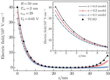
Figure 4 shows the electric field distribution along the channel for the different Ge mole fractions of x = 0.1, x = 0.2, and x = 0.3. This figure describes that the electric field in the lightly doped channel increases as the Ge mole fraction x increases. The maximum point of the electric field is at the source–channel junction, which is attributed to the junction where the tunneling take place. The channel electric field between the source–channel and drain–channel junction remains constant and is approximately zero. Good agreements between the analytical and simulations results are observed.

Fig. 4. Electric field distribution along the channel for the different Ge mole fractions x.

To verify the threshold voltage analytical model, a TCAD simulation was used. The model threshold voltage is extracted using the peak transconductance method. In Figs. 58, the variation of the threshold voltage with the Ge mole fraction x, gate dielectric permittivity, gate oxide thickness, and gate length are shown.

Fig. 5. Variation of threshold voltage with the Ge mole fraction x in Si1−xGex.
Fig. 6. Variation of the threshold voltage with the gate oxide permittivity.
Fig. 7. Variation of the threshold voltage with the oxide thickness.
Fig. 8. Variation of the threshold voltage with the gate length.

Figure 5 illustrates the variation of the threshold voltage with the Ge mole fraction x. We can see that the threshold voltage decreases almost linearly with increasing Ge mole fraction x. This reduction can be attributed to a decrease of the flat-band voltage and the built-in potential barriers in the source-channel or drain-channel junctions, and an increasing tunneling probability of the electrons. The threshold voltage obtained from the analytical model tracks well with the TCAD results.

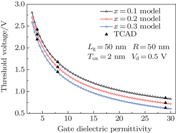
The variation of threshold voltage for different values of gate oxide permittivity and gate oxide thickness with the Ge mole fraction x = 0.1, x = 0.2, and x = 0.3 are shown in Figs. 6 and 7, respectively. Both figures show that the threshold voltage decreases with increasing Ge mole fraction x, which is due to the strain.

In Fig. 6, when the gate oxide permittivity is scaled down from 30 nm to 3 nm, the threshold voltage increases. The reason is that a higher gate oxide permittivity increases the gate control of the tunnel junction, resulting in a decrease of the threshold voltage. Therefore, to achieve the lower threshold voltage in a GAA TFET, usually, a higher gate oxide permittivity is employed. In Fig. 7, the threshold voltage increases linearly as the gate oxide thickness increases. By decreasing the gate oxide thickness, the gate control of the barrier width is increased in the tunnel junction, and it helps to decrease the value of the threshold voltage.

Therefore, in order to obtain improved characteristics of the GAA TFET, a high k material and thinner oxide layer is chosen. The proposed model results coincide well to those of the TCAD simulation results.

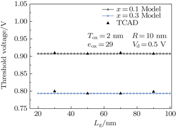
The variation of the threshold voltage with the length of the gate at constant drain and gate voltages is shown in Fig. 8. The threshold voltage curve remains constant when the length of the gate increases. This is due to the fact that the electric field is maximum at the source-channel junction and is independent of the gate length. On the other hand, the channel acts like a resistance in the case of a TFET. If the length of the gate increases, then the channel resistance will increase. Therefore, to reduce the channel resistance, the length of the gate is set to 50 nm.

4. Conclusion and perspectives

In summary, an analytical threshold voltage model that is based on the surface potential and electric field models obtained by solving the 2D polar coordinate Poisson’s equation in the channel for a strained silicon GAA TFET has been developed. Furthermore, it can be observed that the proposed model can predict the trend of the threshold voltage with the key TFET parameters. Our results show that the threshold voltage decreases with increasing Ge mole fraction x, and the gate dielectric permittivity increases with increasing gate oxide thickness. Superior to the MOSFET device, the threshold voltage of the TFET remains constant when the length of the gate increases. Therefore, to obtain improved characteristics of the GAA TFET, a high-k material, and thin oxide layer, and strain for x = 0.3 in Si1−xGex can be chosen. The proposed models provide an effective reference for the design and application of the GAA TFET.

Reference
1Saramekala G KDubey STiwari P K 2015 Chin. Phys. 24 108505
2Kumar SRaj B 2015 J. Comput. Electron. 14 820
3Chander SBaishya S 2015 IEEE Electr. Dev. Lett. 36 714
4Arun Samuel T SBalamurugan N BNiranjana TSamyuktha B 2014 J. Electr. Eng. Technol. 9 655
5Hähnel DFischer IIsemann HOehme MSchulze J2012International Silicon-Germanium Technology and Device MeetingJune 4–6, 2012Berkeley11210.1109/ISTDM.2012.6222483
6Brinda BSrimanta BRajsekhar K2011Annual IEEE India ConferenceDecember 16–18, 2011Hyderabad410.1109/INDCON.2011.6139465
7Luong G VTrellenkamp SZhao Q TMantl S2015Joint International EUROSOI Workshop and International ConferenceJanuary 26–28, 2015Bologna6510.1109/ULIS.2015.7063774
8Zhang JHu H YYang M Y 2015 Acta Phys. Sin. 64 238502 (in Chinese)
9Cui NLiang R RWang JXu J2012International Silicon-Germanium Technology and Device MeetingJune 4–6, 2012Berkeley210.1109/ISTDM.2012.6222412
10Qin S SZhang H MHu H YDai X YXuan R XShu B 2010 Chin. Phys. 19 117309
11Lee MJeon YJung J CKoo S MKim S 2012 Appl. Phys. Lett. 100 253506
12Dash SMishra G P 2015 Superlattices Microstruct. 86 211
13Li Y CZhang H MZhang Y MHu H YWang BLou Y LZhou C Y 2013 Chin. Phys. 22 038501
14Liu YHe JChan W XDu C XYe YZhao WWu WDeng W LWang W P 2014 Chin. Phys. 23 097102
15Boucart KIonescu A M2007Proceedings of the 37th European Solid-State Device Research ConferenceSeptember 11–13, 2007Germany29910.1109/ESSDERC.2007.4430937