Lumped modeling with circuit elements for nonreciprocal magnetoelectric tunable band-pass filter
Li Xiao-Hong, Zhou Hao-Miao†, , Zhang Qiu-shi, Hu Wen-Wen
College of Information Engineering, China Jiliang University, Hangzhou 310018, China


† Corresponding author. E-mail: mailto: zhouhm@cjlu.edu.cn

Project supported by the National Natural Science Foundation of China (Grant Nos. 11172285, 11472259, and 11302217) and the Natural Science Foundation of Zhejiang Province, China (Grant No. LR13A020002).

Abstract
Abstract

This paper presents a lumped equivalent circuit model of the nonreciprocal magnetoelectric tunable microwave band-pass filter. The reciprocal coupled-line circuit is based on the converse magnetoelectric effect of magnetoelectric composites, includes the electrical tunable equivalent factor of the piezoelectric layer, and is established by the introduced lumped elements, such as radiation capacitance, radiation inductance, and coupling inductance, according to the transmission characteristics of the electromagnetic wave and magnetostatic wave in an inverted-L-shaped microstrip line and ferrite slab. The nonreciprocal transmission property of the filter is described by the introduced T-shaped circuit containing controlled sources. Finally, the lumped equivalent circuit of a nonreciprocal magnetoelectric tunable microwave band-pass filter is given and the lumped parameters are also expressed. When the deviation angles of the ferrite slab are respectively 0° and 45°, the corresponding magnetoelectric devices are respectively a reciprocal device and a nonreciprocal device. The curves of S parameter obtained by the lumped equivalent circuit model and electromagnetic simulation are in good agreement with the experimental results. When the deviation angle is between 0° and 45°, the maximum value of the S parameter predicted by the lumped equivalent circuit model is in good agreement with the experimental result. The comparison results of the paper show that the lumped equivalent circuit model is valid. Further, the effect of some key material parameters on the performance of devices is predicted by the lumped equivalent circuit model. The research can provide the theoretical basis for the design and application of nonreciprocal magnetoelectric tunable devices.

1. Introduction

For magnetoelectric composite materials consisted of ferromagnetic and ferroelectric phases, the strain coupling leads to the direct/converse magnetoelectric coupling effect[17] in the magnetoelectric composite materials. The magnetoelectric composite materials and multiferroic film possess the capability of controlling magnetism and the ability of tuning ferromagnetic resonance by an electric field applied to the piezoelectric phase through magnetoelectric (ME) coupling.[813] Due to the magnetization controlled by the electrostatic field or voltage, the magnetoelectric coupling mechanism may contribute to the formation of a series of RF/microwave magnetoelectric devices[1416] in the future, whose frequency and bandwidth are magnetoelectric tunable. At present, the magnetoelectric tunable filter,[17,18] the magnetoelectric resonator,[19,20] the magnetoelectric phase shifter,[2124] and antenna[2527] are representative. The traditional frequency agility device can be formed by the electrostrictive and magnetostrictive materials. However, these devices tend to be bulky, in slow speed of adjustment, have large energy consumption, and can only work within a narrow band. The new adjustable magnetoelectric RF/microwave devices will not only dramatically improve the design method of the military RF/microwave radio and radar, but also will greatly enhance the competitiveness of the consumer electronics industry.

According to the direction of the magnetic field and the direction of the wave vector, magnetostatic waves can be divided into magnetostatic surface waves and magnetostatic forward/backward volume waves. Because the magnetostatic surface wave has low transmission loss and the nonreciprocal transmission characteristic on the upper and lower surfaces of the ferrite slab, and contributes to the design of nonreciprocal devices.[28] At present, there are many studies into the transmission characteristics of magnetostatic surface waves and the application of microwave devices.[29] The common nonreciprocal ferrite devices are mostly multiport, such as the isolator, the circulator and the directional coupler,[3033] and the frequency band usually does not have the adjustability. Therefore, Wu et al.[34] firstly changed the placement angle of ferrite slab in two inverted L-shaped microstrip lines and put forward a microwave band-pass filter which has nonreciprocity and adjustability of magnetic field.

Using the magnetoelectric composite materials composed of ferrite and ferroelectric materials, magnetoelectric microwave devices which have nonreciprocity and magnetoelectric adjustability have been successfully designed. For the design of microwave devices containing ferrite or magnetoelectric materials, the electromagnetic field simulation is a kind of important mean. However, due to the introduction of functional materials, the electromagnetic field simulation is time-consuming and has low-efficiency. The lumped equivalent circuit method, which is applied for the aided analysis of the performance of microwave devices, can greatly improve the designed efficiency. Marcelli et al.[35,36] firstly proposed the equivalent circuit model of the magnetostatic wave straight edge resonator. After Tsai et al.[37] established the equivalent circuit model of the double stop-band filter which consisted of two cascaded band-stop filters. In recent years, for the reciprocal dual-tunable microwave magnetoelectric device, Zhou et al.[3841] treated the voltage of the piezoelectric layer as a magnetic field and established the lumped circuit models of the direct conduction band, the coupled band and T-type magnetoelectric microwave devices, which greatly promoted the application of the equivalent circuit model. However, the above lumped equivalent circuit models focus on the reciprocal two-port devices, and the lumped equivalent circuit model of nonreciprocal frequency band tunable microwave devices is not correlatively researched.

In this paper, considering transmission characteristics of magnetostatic waves of the filter, the lumped equivalent circuit model of a nonreciprocal magnetoelectric tunable band-pass filter is established, which is consisted of the reciprocal coupled band circuit and the nonreciprocal T-shaped circuit. The comparison of the predicted results and the experimental results of S parameters in the reciprocal and nonreciprocal cases confirms the validity of the established lumped equivalent circuit model. Then, the electric tunable performance of the magnetoelectric tunable filter, the impact of the thickness of ferrite slab and the width of the coupled microstrip line on devices are separately predicted by the lumped equivalent circuit model. It is found that these key parameters have a very significant effect on the band-pass center frequency, bandwidth, and the isolation, so the lumped equivalent circuit model will benefit the design and application of new microwave devices which have nonreciprocity and magnetoelectric adjustability.

2. The nonreciprocal ME tunable filter

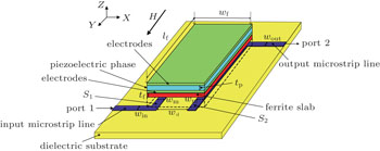
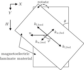
A typical reciprocal magnetoelectric (ME) tunable band-pass filter is shown in Fig. 1, which consists of the laminated ME composites, the dielectric substrate, and two inverted L-shaped microstrip lines. Laminated ME composites are composed of piezoelectric and ferromagnetic phases. The ferrite is selected as the ferromagnetic phase with the dimensions lf × wf × tf and saturation magnetization Ms. The piezoelectric material with the thickness tp is selected as the ferroelectric phase, and the piezoelectric material has the same length and width as the ferromagnetic phase. Two metal films used as electrodes are plated on both sides of the piezoelectric material in order to apply the external electric field E to the piezoelectric material. The dielectric material with the thickness ta is selected as the substrate. For two L-shaped microstrip lines, microstrip lines along the x direction are respectively defined as the input microstrip line and the output microstrip line, which have the same thickness tm, and the widths are respectively win and wout. The input and output ports and the dielectric substrate satisfy the matched characteristic impedance of 50 Ω. Two microstrip lines along the y direction are respectively defined as the coupled microstrip lines S1 and S2, which have the same width wm and thickness tm. The distance between S1 and S2 is wd. The external magnetic field H is applied along the y direction. The laminated ME composites are placed in the two L-shaped microstrip lines, wherein the longitudinal direction of the laminated ME composites is along the y direction (as shown in Fig. 1). Then the reciprocal ME band-pass filter is formed, that is, the S parameter curve of the situation where the signal is inputted from port 1 and outputted from Port 2 is consistent with that of the opposite situation. When ME laminated structure is rotated by an angle θ in the xy plane (see Fig. 2, θ ∈ (0,45°)), the S parameter curve of the situation where the signal is inputted from port 1 and outputted from port 2 is different from that of the opposite situation. Therefore, a novel nonreciprocal ME tunable filter is formed when the ME laminated structure is rotated by an angle θ in Fig. 1.

Fig. 1. Schematic structure of the reciprocal ME tunable band-pass filter.
Fig. 2. Schematic diagram of the rotated ME laminated structure.

For the nonreciprocal ME tunable band-pass filter, when the external magnetic field H is applied along the direction parallel to the plane of microstrip lines (i.e., the y direction in Fig. 1), the ferromagnetic resonance phenomenon is produced by ferrite materials. Considering the anisotropic magnetic field Han and demagnetizing field Hdem, the effective inside magnetic field of ferrite materials is H0 = H + Han + Hdem. Obviously, the effective inside magnetic field has been changed due to the changed external magnetic field and then the ferromagnetic resonance frequency (FMR) has also been changed. Then the bandwidth of the nonreciprocal ME tunable filter formed in Figs. 1 and 2 has been ultimately adjusted. When the piezoelectric layer is spliced onto the ferrite layer, the ME laminated composite is formed. The external electric field is applied to the piezoelectric layer to generate the in-plane stress produced by the inverse piezoelectric effect, the in-plane stress will be transferred to the piezomagnetic layer through the binding effect of the laminate structure, and then magnetic performance of the piezomagnetic layer will be changed. That is to say the applied external electric field changes the ferromagnetic resonance frequency of the piezomagnetic layer. Therefore, an equivalent magnetic field δHE = AE is introduced to describe the change, where A is the ME voltage coefficient. Meanwhile, the effective inside magnetic field H0 of the ferrite includes the DC bias magnetic field, the anisotropic magnetic field, the demagnetizing field, and the equivalent magnetic field induced by the converse magnetoelectric effect, namely, H0 = H + Han + Hdem + δHE. Obviously, when the external electric field varies, the effective magnetic field is correspondingly changed. Therefore, the ferromagnetic resonance frequency and working frequency range of the nonreciprocal ME filter will be changed.

According to the electrically tunable FMR frequency shifting model established by Zhou et al.,[13] a concise expression of the coefficient A is written as

where λs represents the saturation magnetostriction constant; pd31, pS11, and pS12 are material parameters of the piezoelectric layer; mS11 and mS12 are material parameters of the piezomagnetic layer; and kc is the coupling coefficient. For the nonreciprocal magnetoelectric resonator formed in Figs. 1 and 2, an electromagnetic wave signal is inputted from port 1, which firstly transmits on the input microstrip line and then transmits on the microstrip line S1. When the external magnetic field H is applied to the piezomagnetic layer along the y direction or the electric field H is applied to the piezoelectric layer, the magnetostatic surface wave is generated and then transmits under the joint action of the external magnetic field and electromagnetic waves. When the lower surface wave transmits to the other side, the magnetostatic surface wave transmits along the y direction due to the reflex action of hypotenuse of the ferrite, and magnetostatic backward volume waves are generated, namely, the magnetostatic surface wave and magnetostatic backward volume waves are simultaneously generated. For the magnetostatic surface wave, when the magnetostatic lower surface wave transmits to the hypotenuse along the direction of the x axis, magnetostatic upper surface waves are restrained owing to reflex action. When θ = 45°, the restraining action reaches the maximum. Therefore, the magnetostatic surface wave could not form a circular wave, which results in the nonreciprocal characteristic of the filter. Meanwhile, k+ and k respectively are the wave numbers of magnetostatic upper and lower surface waves in the ferrite slab and meet the following equations:

When θ = 0°, the magnetostatic surface wave is induced in the ferrite slab and transmits along the lower surface of ferrite slab. The magnetostatic surface wave is reflected on the other straight edge of the ferrite slab and transmits along the upper surface of the ferrite slab. Then the upper surface wave and lower surface wave form a circular wave. Meanwhile, due to the coupling effect between the magnetostatic surface wave and microstrip line S2, the magnetostatic surface wave is translated into the electromagnetic wave, transmits on the microstrip line and the output microstrip line, and then is outputted through the output port. When θ = 0° in Eq. (2), k+ and k are the wave numbers of the upper and lower surface waves of the reciprocal ME device and meet the following equation:

The transmission characteristic of the magnetostatic wave mainly depends on the mode of wave. The transmission characteristic is related with the included angle φ between the normal vector n of the external magnetic field and the vector k of the transmissive wave. As is shown in Fig. 2, kl,fwd and kw,fwd are the components of the lower surface wave in the length and width directions, kl,bwd and kw,bwd are the components of the upper surface wave in the length and width directions. Meanwhile, the included angles φ between the vector n and four components are respectively 90° + θ, 180° −θ, 90° −θ, and θ. Therefore, the dispersion equation[42] is as follows:

where

ω represents the angular frequency; ω0 = −γH0, and ωm = −γ4πMs; γ = 2.8 MHz/Oe is the gyromagnetic ratio. Obviously, the amplitude of the wave vector is k = k+ = k according to Eq. (2). Then k is substituted into Eq. (4) and the effective magnetic field H0 induced by the external magnetic field and electric field is also substituted into Eq. (4). Ultimately, the shifting amount of the FMR angular frequency ω is obtained for the ME nonreciprocal filter.

3. The lumped models of nonreciprocal ME tunable filter

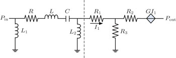
The nonreciprocal ME tunable filter is shown in Figs. 1 and 2 and the nonreciprocal characteristic of the filter depends on the deviation angle θ of the ME laminated material. When θ = 0°, the nonreciprocal ME tunable device is degraded into the reciprocal ME tunable device. Therefore, it is convenient for the establishment of the lumped equivalent circuit model for nonreciprocal ME tunable filter that the lumped equivalent circuit is decomposed into a lumped circuit unit of the reciprocal device and a lumped circuit unit which reflects the nonreciprocal characteristic. According to the research of Zhou et al.,[39] the reciprocal coupling ME device is shown in Fig. 1. The different coupling inductances are introduced to indicate the coupling effect among the ferrite layer, the input and output microstrip lines, and then a typical RLC resonance circuit is used to describe the FMR effect induced by the electromagnetic wave via the ferrite layer. Ultimately, a simple Π-shaped lumped equivalent circuit is established to describe the reciprocal ME device (a Π-shaped lumped circuit is shown on the left side of the dashed line of Fig. 3). Subsequently, according to the microwave engineering, a T-shaped lumped circuit with the controlled sources can be used to describe the nonreciprocal characteristic (a T-shaped lumped circuit is shown on the right side of the dashed line of Fig. 3). Therefore, combining a Π-shaped lumped circuit of the reciprocal device and a T-shaped lumped circuit of the nonreciprocal unit, a concise lumped equivalent circuit model of nonreciprocal ME tunable filter is established (see Fig. 3).

Fig. 3. The lumped equivalent circuit model of the nonreciprocal ME tunable band-pass filter.

For the reciprocal coupling circuit, the radiation impedance per unit length is introduced to indicate the interaction between the magnetostatic wave and the electromagnetic wave according to the interaction principle between the magnetostatic wave and the electric current. Therefore, the radiation impedance per unit length[34] is written as

where μ0 is the vacuum permeability, μ1 = 1 + χ, v = +1, and v = −1, respectively represent the positive direction and the negative direction of x axis, F = IeksJ0 (kwm/2) denotes the array factor for the current flowing on microstrip lines. Where J0 is the Bessel function of zeroth-order; wm is the width between the microstrip lines S1 and S2; and s is the vertical spacing between the transmission line and ferrite interface. Obviously, the FMR angular frequency ω is solved by Eq. (4).

For the effective length of the microstrip line covered by ferrite slab, the total radiation impedance is calculated by the unit element integration principle and is written as

where l is the length of the microstrip line covered by ferrite slab, which changes with the deviation angle θ; ; εr represents the permittivity of the substrate.

After the radiation impedance is obtained, and RLC series resonant circuit, which contains the radiation inductance L and the radiation capacitance C, is introduced to indicate the inside FMR effect of the ferrite. The unloaded quality factor Q0 = f0/(γΔH) is obtained by the resonance line width ΔH, and then the radiation impedance and the radiation capacitance are got by the definition of the unloaded quality factor of the series resonant circuit. But Marcelli et al.[35] pointed out that the coupling effect between microstrip lines and the laminated ME composites is necessarily considered to get the effective radiation inductance and radiation capacitance when the ferrite layer is located in the middle of two microstrip lines. Therefore, the coupling factor k1 = (2/Qext)exp(−kD) is introduced to describe the coupling effect between microstrip lines and the laminated ME composites, where D is the distance between the ferrite layer and the current flowing on the microstrip line; Qext is the external quality factor[36] and is written as

where K = ln[(wm + tm + 2ta)/(wm + tm)]/4ta; Z0 is the characteristic impedance; ωM = 4πγMs; and Veff is the volume of ferrite layer. In the establishment process of the model, the input and output ports exist in the reciprocal characteristic for the reciprocal coupling circuit, and then Qext = Qext,1 = Qext,2 is obtained. In a particular case, when the filter meets the electric matching, the coupling factor is written as

so the equivalent capacitance and inductance are modified as

Meanwhile, the coupling inductances L1 and L2 are used to describe the coupling effect between microstrip lines and ferrite slab in Fig. 3. The expression is written as

Therefore, the lumped equivalent circuit is established for the reciprocal ME device on the left side of the dashed line of Fig. 3 according to Eqs. (6) and (9)–(11).

For the nonreciprocal lumped circuit shown on the right side of the dashed line of Fig. 3, the electromagnetic wave signal passes through the input microstrip line and then transmits on the microstrip line S1 along the y direction. Furthermore, the magnetostatic wave transmits on the ferrite slab and then transmits on the microstrip line S2 by the coupling effect. Obviously, R1 and R2 in the right parts of the dashed lines are independent of the magnetic field and the electric field and are the impedances of the electromagnetic wave which transmits on the microstrip lines S1 and S2. Because the widths of the microstrip lines S1 and S2 are the same and the thicknesses of S1 and S2 are also the same. Therefore, according to the symmetry, R1 = R2 is known and the expression is written as

where εe is the effective permittivity of the microstrip line and εr is the relative permittivity of the substrate.

When the deviation angle θ is zero, the upper and lower magnetostatic surface waves circularly transmit and the device is reciprocal. When the deviation angle θ is non-zero, magnetostatic backward volume waves are generated due to the reflection action of the hypotenuse. Nevertheless, the magnetostatic backward volume wave cannot be returned, so the nonreciprocal characteristic is generated. Therefore, the radiation impedance R3 of the lumped equivalent circuit is the impedance of magnetostatic backward volume waves transmitting on the ferrite slab. According to the direction shown in Fig. 2, the relationship between the radiation impedance R3 and the radiation impedance of magnetostatic backward volume waves transmitting on the lower surface of ferrite slab along the x direction is the cotangent,

The gain G of the nonreciprocal unit in Fig. 3 indicates the difference between the radiation impedance generated by the electromagnetic wave inputted from port 1 and the radiation impedance generated by the electromagnetic wave outputted from port 2. Therefore, the expression is written as

Equations (12)–(15) are lumped parameters of the nonreciprocal unit in Fig. 3, equations (6), (9)–(11) are lumped parameters of the reciprocal unit in Fig. 3, and then a lumped equivalent circuit model of a nonreciprocal ME tunable band-pass filter is finally established. Further, the external electric field, the magnetic field, the size of the device, and material parameters are substituted into the established model, and the performance of the device is easily analyzed by the lumped equivalent circuit model shown in Fig. 3.

4. Results and discussion

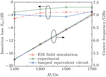
In order to verify the validity of the lumped equivalent circuit model, the experimental results of the magnetic tunable microwave filter in Ref. [34] were selected as the reference. Wherein the YIG slab is selected as the ferrite material, the dimension lf × wf × tf is 3.6 mm × 2 mm × 0.108 mm, and the saturation magnetization is 4πMs = 1750 G. The widths of the input and output microstrip lines are win = wout = 0.37 mm, the width of the coupled microstrip line is wm = 0.32 mm, the distance between the microstrip line S1 and microstrip line S2 is wd = 1.2 mm, and the deviation angle is 45°. Here, the length of the microstrip line covered by YIG slab is about 2.5 mm, the dielectric substrate is Rogers TMM 10i, the thickness is 0.381 mm, the dielectric constant is εr = 9.8, and the loss angle tangent is tan δ = 0.002. For the nonreciprocal magnetic tunable microwave filter, the electric field is only taken as 0 in the expression of the effective magnetic field H0 of the lumped equivalent circuit model, which is shown in Fig. 3. Now, the predicted results of the lumped equivalent circuit model and the electromagnetic field simulation and the experimental results of the nonreciprocal magnetic tunable filter are compared as shown in Fig. 4. As can be seen from Fig. 4, the predicted center frequency and the predicted insertion loss values are qualitatively in good agreement with the experimental results, when the static magnetic field is set to 1100 Oe, 1300 Oe, 1500 Oe, and 1700 Oe. In order to analyze the predicted results more clearly, the predicted center frequency of Fig. 4 and the predicted insertion loss of the center frequency point and the experimental results are shown in Fig. 5. From Fig. 5, it can be found that the predicted results of the lumped equivalent circuit and the electromagnetic field simulation are basically consistent in the central frequency point. The deviations of the predicted results and experimental results are about 10 MHz. In terms of the maximum insertion loss, the predicted results of the lumped equivalent circuit and the electromagnetic field simulation are basically consistent, which are smaller 2 dB than the experimental results. In summary, the predicted results of the lumped equivalent circuit model and the electromagnetic field simulation are in good agreement with the experimental results. Therefore, the validity of the lumped equivalent circuit model is verified.
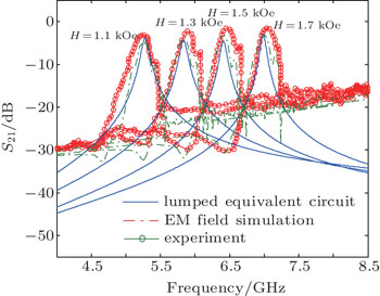
Fig. 4. The contrast diagram of the predicted insertion loss curves of the lumped equivalent circuit model and the experiment values for the deviation angle 45°.
Fig. 5. The contrast diagram of the predicted insertion loss S21 and the predicted center frequency and the experiment values under different magnetic fields.

Meanwhile, the insertion loss S12 predicted by the equivalent circuit model is compared with the experimental results in Fig. 6 (in order to improve the recognition degree, the results of electromagnetic field simulation are not placed in Fig. 6). When the magnetic field changes from 1100 Oe to 1700 Oe, the maximum insertion loss obtained by the equivalent circuit model is below −15 dB, which has a high isolation degree and can achieve the same isolation effect as the experimental results. From Figs. 46, the lumped equivalent circuit model can effectively predict the basic characteristics of the nonreciprocal filter.
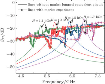
Fig. 6. The contrast diagram of the predicted insertion loss S12 of the lumped equivalent circuit model and the experiment values for the deviation angle 45°.

Keep the thickness tf = 0.108 mm of YIG unchanged, adjust the deviation angle of YIG to be 0°. Then magnetostatic upper surface waves will not be suppressed and this filter will present the reciprocal characteristics from the above analysis. Exploiting the experimental results[34] in the reciprocal case, the comparison results of the S21 curve and the S12 curve obtained by the lumped equivalent circuit model and the experimental results are respectively shown in Figs. 7(a) and 7(b) in the magnetic field 1600 Oe. As can be seen from Figs. 7(a) and 7(b), the S21 and the S12 curves, the center frequency and the insertion loss of the center frequency, which are obtained by the lumped equivalent circuit model and the electromagnetic field simulation, are in good agreement with the experimental results and can effectively describe the reciprocal characteristic of the device. The band-pass ripple of the experimental insertion loss is smaller, the predicted curve obtained by the lumped equivalent circuit model is relatively smooth, and the predicted curve of the electromagnetic field simulation has a larger ripple. From this point of view, the lumped equivalent circuit model is better than the electromagnetic field simulation. Meanwhile, from Figs. 47, it can be seen that the model can well describe the experimental results of the nonreciprocal magnetoelectric tunable microwave bandpass filter (see Figs. 46) and also describe the experimental results under the degenerated reciprocal condition (see Fig. 7). In fact, when the model degenerates into the reciprocal model, the degenerated equivalent circuit is consistent with the model of Ref. [39]. Therefore, the research work of this paper extends the lumped circuit model of the reciprocal microwave magnetoelectric device to more general nonreciprocal devices and provides a theoretical basis for the design and application of the nonreciprocal magnetoelectric microwave devices in high performance.
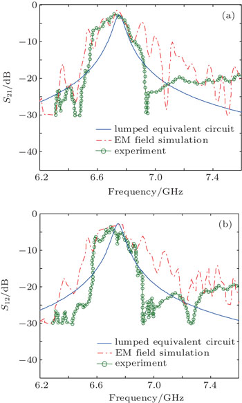
Fig. 7. The contrast diagram of the predicted insertion loss S21 (a) and S12 (b) of the lumped equivalent circuit model and the experiment values for the deviation angle 0°.

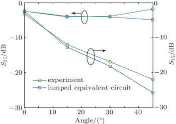
For the validity of the equivalent circuit model at the different deviation angles of ferrite slab, the experimental results in Ref. [34] are still selected. Select the 0.5 mm thick YIG slab and change the included angle between the YIG slab and the y axis to do the prediction by the model. Keeping the bias magnetic field H = 1600 Oe unchanged, the impact of the reflecting hypotenuse on the backward surface wave and the S parameter gradually increases when the deviation angle changes from 0° to 45°. As shown in Fig. 7, the S21 curve is basically consistent with the S12 curve when the deviation angle is 0°. When the deviation angle gradually increases, the nonreciprocal characteristic gradually appears according to the above analysis. When the deviation angle is 45°, the nonreciprocal characteristic becomes the most obvious. By changing the placement angle of the YIG slab, the comparison of the predicted results obtained by the lumped equivalent circuit model and the experimental results is shown in Fig. 8. As can be seen from Fig. 8, the insertion loss S21 and S12 curves obtained by the equivalent circuit model are qualitatively in good agreement with the experimental results and can well reflect the nonreciprocal characteristic which increases with the increase of the deviation angle.

Fig. 8. The insertion loss S21 and S12 curves under the influence of deviation angles.

An equivalent magnetic field is introduced to describe the applied electric field on the piezoelectric layer adjusting the frequency band of devices, and then the lumped parameters of the lumped equivalent circuit model are calculated under the condition of the applied voltage. Choose PZT as the piezoelectric layer, substitute the material parameters into the magnetoelectric conversion coefficient in Ref. [13], and then get the magnetoelectric conversion coefficient A = 5.2 Oe·cm·kV−1 (i.e., the applied electric field can be equivalent to δHE = 5.2E). After the external bias field 1600 Oe remains unchanged, figure 9 shows the device performance predicted by the lumped equivalent circuit model and the electromagnetic simulation when the external electric field varies from −10 kV/cm to 10 kV/cm at the two ends of piezoelectric layer. As can be seen from Fig. 9(a), the S21 curves obtained by the equivalent circuit model and the electromagnetic field simulation are qualitatively consistent at the center frequency point under different electric fields. The bandwidth obtained by the electromagnetic field simulation is wider than that obtained by the lumped equivalent circuit model, because the given boundary conditions of the device are more close to the actual situation in the electromagnetic field simulation. The S12 curves obtained by the lumped equivalent circuit model and the electromagnetic field simulation are shown in Fig. 9(b). As can be seen from Fig. 9(b), the insertion loss S12 is below −12 dB under different electric fields and has a distinct band-stop characteristic. Therefore, it can be found that the electric field can adjust the working frequency of the device and the nonreciprocal characteristic still exists in Fig. 9.
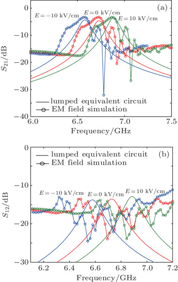
Fig. 9. The insertion loss S21 (a) and S12 (b) curves under different electric fields (for the deviation angle 45°).

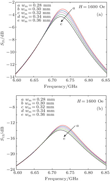
Next, the designed nonreciprocal device has several important parameters, such as the thickness of ferrite layer and the width of the coupled microstrip lines, and the impact of several important parameters on the performance of the device is predicted. Firstly, considering the impact of the thickness of ferrite layer, keep static magnetic field H = 1600 Oe unchanged, and the thickness of YIG slab changes from 0.008 mm to 0.5 mm. The insertion loss S21 and S12 curves predicted by the lumped equivalent circuit model are shown in Fig. 10. When the thickness changes from 0.008 mm to 0.2 mm, the S21 curve is easily influenced by the thickness and the center frequency sharply increases in Fig. 10(a) (the increments are approximately 500 MHz). When the thickness changes from 0.2 mm to 0.5 mm, the center frequency of the S21 curve becomes gradually smaller, but the change is relatively small. As can been seen from Fig. 10(b), the isolation degree becomes gradually low and the isolation degree at the center frequency has been greater than −10 dB in the 0.2 mm thickness when the thickness changes from 0.008 mm to 0.2 mm. When the thickness continuously increases and then the isolation degree rapidly decreases. Figures 10(a) and 10(b) show that ferrite layer with the optimal thickness can improve the band-pass effect and also increase the isolation degree.
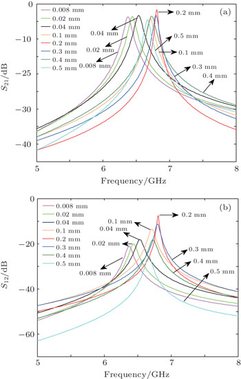
Fig. 10. The insertion loss S21 (a) and S12 (b) curves under different thicknesses of YIG (for the deviation angle 45°).

The insertion loss curves predicted by the equivalent circuit model are shown in Fig. 11 under the different widths of the coupled microstrip line. As can be seen from Fig. 11(a), the maximum insertion loss S21 gradually decreases with the increase of the width of the microstrip line resulting in the difference of 2 dB. Because the increase of the width of the microstrip line leads to the decrease of the radiation impedance, and the coupling effect between ferrite slab and the microstrip line becomes weak resulting in the decrease of the insertion loss. Meanwhile, the center resonant frequency slightly offsets to the left and the drift amount remains unchanged. With the increase of the width, the insertion loss gradually decreases and the isolation effect becomes better.

Fig. 11. The insertion loss S21 (a) and S12 (b) curves under different widths of the coupled microstrip line (for the deviation angle 45°).
5. Conclusion

In this paper, for the nonreciprocal magnetoelectric dual tunable microwave band-pass filter, a lumped equivalent circuit model is established, which is based on the lumped equivalent circuit of the reciprocal coupled band-pass filter and the introduced nonreciprocal circuit with the controlled sources. Change the deviation angle of YIG slab to make the device respectively be in the reciprocal and nonreciprocal case. For the S21 curve predicted by the equivalent circuit model, its band-pass frequency, bandwidth, and the insertion loss are in good agreement with the experimental results. The predicted and measured insertion loss S12 results are below −15 dB under the nonreciprocal state, which have a higher isolation degree. Then, based on some important parameters of the nonreciprocal device, the lumped circuit model is used to do the prediction. It is found that the thickness of the ferrite layer has a complex effect on the center frequency and the isolation degree. YIG slab with the optimal thickness may simultaneously enhance the band-pass effect and the isolation degree. The width of the coupled microstrip line monotonically impacts on the device performance and the insertion loss S21 and S12 monotonically decrease with the increase of the width of the microstrip line.

Reference
1Nan C WBichurin M IDong S XViehland DSrinivasan G 2008 J. Appl. Phys. 103 031101
2Eerenstein WMathur N DScott J F 2006 Nature 442 759
3Ma JHu J MLi ZNan C W 2011 Adv. Mater. 23 1062
4Zhou H MLi CXuan L MWei JZhao J X 2011 Smart Mater. Struct. 20 035001
5Zhou H MOu X WXiao YQu S XWu H P 2013 Smart Mater. Struct. 22 035018
6Zhou H MCui X L 2014 J. Appl. Phys. 115 083905
7Zhou H MCui X L 2014 Smart Mater. Struct. 23 105014
8Liu MSun N X 2014 Phil. Trans. R. Soc. 372 20120439
9Liu MLou JLi S DSun N X 2011 Adv. Funct. Mater. 21 2593
10Liu MHowe B MGrazulis LMahalingam KNan T XSun N XBrown G J 2013 Adv. Mater. 25 4886
11Liu MZhou Z YNan T XHowe B MBrown G JSun N X 2013 Adv. Mater. 25 1435
12Zhou Z YPeng BZhu M MLiu M 2016 J. Adv. Dielectrics 6 1630005
13Zhou H MChen QDeng J H 2014 Chin. Phys. 23 047502
14Yang XZhou ZNan TGao YYang G MLiu MSun N X 2016 J. Mater. Chem. 4 234
15Ciomaga C EAvadanei O GDumitru IAirimioaei MTascu STufescu FMitoseriu L 2016 J. Phys. D: Appl. Phys. 49 125002
16Lin HGao YWang X JNan T XLiu MLou JYang G MZhou Z YYang XWu JLi MHu Z QSun N X 2016 IEEE Trans. Magn. 52 4002208
17Yang XGao YWu JBeguhn SNan TZhou ZLiu MSun N X 2013 IEEE Trans. Magn. 49 5485
18Tatarenko A SGheevarughese VSrinivasan GAntonenkov O VBichurin M I 2010 J. Electroceram. 24 5
19Ustinov A BTiberkevich V SSrinivasan GSlavin A N 2006 J. Appl. Phys. 100 093905
20Ustinov A BSrinivasan GFetisov Y K 2008 J. Appl. Phys. 103 063901
21Ustinov A BSrinivasan GKalinikos B A 2007 Appl. Phys. Lett. 90 031913
22Tatarenko A SSrinivasan G 2011 Microw. Opt. Technol. Lett. 53 261
23Yang G MSun N X 2014 IEEE Trans. Magn. 50 4005004
24Yang XWu JGao YNan T XZhou Z YBeguhn SLiu MSun N X 2013 IEEE Trans. Magn. 49 3882
25Petrov R VTatarenko A SPandey SSrinivasan G 2008 Electron. Lett. 44 506
26Yang G MXing XDaigle ALiu MObi OWang J WNaishadham KSun N X 2008 IEEE Trans. Magn. 44 3091
27Yang G MXing XDaigle AObi OLiu MLou JStoute SNaishadham KSun N X 2010 IEEE Trans. Antennas Prop. 58 648
28Queck C KDavis L E 2002 IEEE Trans. Microw. Theory Tech. 50 2910
29Adam J DDavis L EDionne G FSchloemann E FStitzer S N 2002 IEEE Trans. Microw. Theory Tech. 50 721
30El-Sharawy E BGuo J S1995IEEE MTT-S International Microwave Symposium Digest1107
31Cao MPietig R 2005 IEEE Trans. Microw. Theory Tech. 53 2572
32Queck C KDavis L E 2004 IEEE Trans. Microw. Theory Tech. 52 625
33Okubot KTsutsumiz M 2003 IEEE MTT-S International Microwave Symposium Digest 1 425
34Wu JYang XBeguhn SLou JSun N X 2012 IEEE Trans. Microw. Theory Tech. 60 3959
35Marcelli RRossi MGasperis P D 1996 IEEE Trans. Magn. 32 4156
36Bartolucci GMarcelli R 2000 J. Appl. Phys. 87 6905
37Tsai C SQiu GGao H LYang L Wet al. 2005 IEEE Trans. Magn. 41 3568
38Zhou H MLi CZhu F JQu S X 2013 J. Appl. Phys. 114 083902
39Zhou H MZhu F J 2013 J. Appl. Phys. 114 153904
40Zhou H MLian J 2014 J. Appl. Phys. 115 193908
41Zhou H MLian JZhu F J 2014 J. Appl. Phys. 116 063904
42Wu JYang XLou JBeguhn SSun N X2012IEEE MTT-S International Microwave Symposium6259689