† Corresponding author. E-mail:
Fluorine plasma treatment was used prior to the Schottky metal deposition on the undoped Al0.45Ga0.55N, which aimed at the solar-blind wavelength. After fluorine plasma treatment and before depositing the Ni/Au Schottky, the samples were thermal annealed in the N2 gas at 400 °C. The reverse leakage current density of Al0.45Ga0.55N Schottky diode was reduced by 2 orders of magnitude at −10 V. The reverse leakage current density was reduced by 3 orders of magnitude after thermal annealing. Further capacitance–frequency analysis revealed that the fluorine-based plasma treatment reduces the surface states of AlGaN by one order of magnitude at different surface state energies. The capacitance–frequency analysis also proved that the concentration of carriers in AlGaN top is reduced through fluorine plasma treatment.
Wide band gap material AlGaN has attracted a great deal of attention for its application in devices such as ultraviolet light emitting diodes (UVLEDs) and ultraviolet photo detectors (UVPDs).[1–3] With the Al content increase from 0 to 1, the band gap of AlxGa1−xN changes from 3.4 eV to 6.2 eV (corresponding to the wavelength from 365 nm to 200 nm). The solar-blind AlGaN UVPDs, with a cut-off wavelength λc ≤ 280 nm, have many applications in missile threat detection, flame monitoring, and biological detection. Schottky AlGaN solar-blind PD is popular for its simple fabrication, fast response, and the use in array photodetectors. However, it suffers from the high dark current due to the high density of dislocations of AlGaN thin film with Al content ≥ 40% and surface defects, which as a result increases the device noise and influences the performance of Schottky photodetectors.[4]
Recently, it has been reported that the fluorine-based plasma treatment fabricated E-mode AlGaN/GaN high-electron-mobility transistors (HEMTs) form a conventional D-mode HEMT structure. The impacts about fluorine treatment on GaN Schottky contact have been reported.[5] However, the effects of Fluorine plasma treatment on high Al content AlGaN and especially the change of surface states after treatment are still unknown.
In this paper, the CHF3 fluorine plasma treatment was used prior to the Schottky metal deposition. We performed the thermal anneal after fluorine plasma treatment before depositing the Ni/Au Schottky.
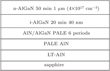
All samples used in this work were grown by a plasma-assisted molecular beam epitaxy system (SVTA) with conventional Knudsen cells for metal sources and radio frequency plasma sources for active nitrogen species. The AlGaN thin films were grown on a thick AlN template prepared by metalorganic chemical vapour deposition (MOCVD) on the sapphire substrate. The structure consisted of a 1000-nm-thick Si-doped Al0.45Ga0.55N layer on top of a 400-nm-thick unintentionally doped n-type Al0.45Ga0.55N. The structure of the samples is shown in Fig.
Firstly, wafer was cleaned by the conventional organic cleaning process, then Ohmic contacts were formed by standard photolithography on AlGaN surface, using a Ti/Al/Ni/Au (30 nm/175 nm/35 nm/100 nm) metal layer annealed at 850 °C in N2 for 35 s in a rapid thermal annealing system. The linearity of Ohmic contact was checked by I–V measurement before the next processing. The samples were divided into four groups (A, B, C, D). Prior to the deposition of the Ni/Au (10/10 nm) Schottky contact metals on the AlGaN, samples B and C were treated by CHF3 using inductive coupled plasma (RIE-ICP) while samples A and D were taken as control. Samples C and D were annealed in the N2 atmosphere at 400 °C. The process of the four samples is summarized in Table
| Table 1. Process of samples. . |
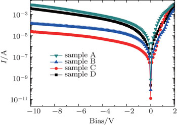
The I–V characteristics of AlGaN Schottky diode with and without fluorine plasma treatment and annealed are shown in Fig.
For thermionic emission (V >3 kT/q), the general diode equation is[6]


Assume that a = nkT/q, b = 1/Is, and c = Rs. The parameters n, Is, and Rs can be deduced from the nonlinear fitting method.
| Table 2. Parameters of AlGaN Schottky diode. . |
As shown in Table
Nitrogen vacancy has been researched for a long time. It not only forms in the growth natively (especially in metal-rich growth conditions) but also could be produced by the processing steps of fabricating devices, such as high-temperature thermal annealing of Ohmic contact, activation of implanted dopants, and plasma induced damage. It is commonly thought that N vacancy is a shallow donor in GaN and AlGaN, which could lower the barrier height and cause excess leakage current in GaN and AlGaN Schottky diodes.[7,8]
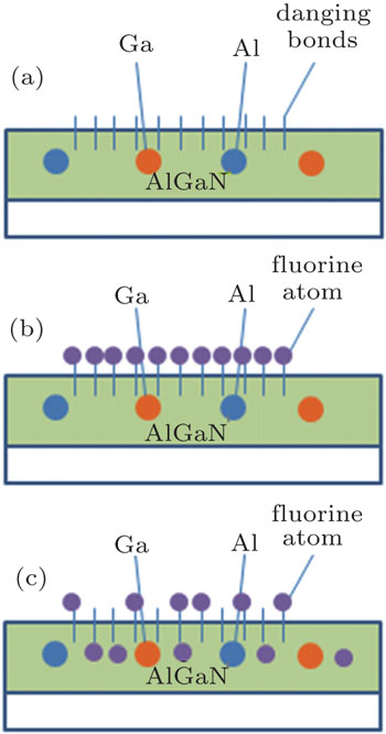 | Fig. 3. Schematic diagram of (a) nitrogen vacancy, (b) fluorine-based plasma treatment, and (c) fluorine-based plasma treatment and annealed. |
In this work, the fluorine-based treatment by RIE-ICP in our experiments has a slight etching effect on AlGaN. We think that the fluorine-based plasma treatment effectively reduces the leakage current by reducing the nitrogen vacancy rather than forming the insulating layer. We give the following model to explain the I–V results. Surface states which are due to the nitrogen vacancy existing on the AlGaN surface are shown in Fig.
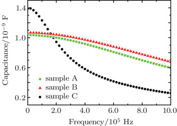
To further verify our postulation, we researched the capacitance–frequency characteristic and the result is shown in Fig.
We analyzed the surface states of the AlGaN Schottky diode with and without fluorine-based plasma treatment. As the surface states contribute to the capacitance of the diode only at the low frequency, the capacitance depending on the frequency is as follows:


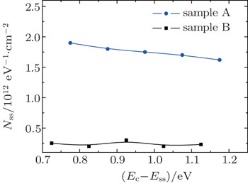
The surface state density of the diode can be obtained by


Figure
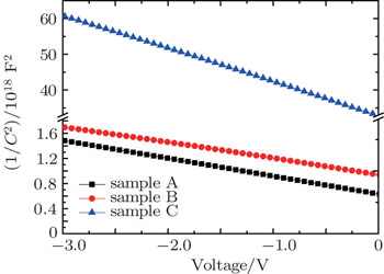
To prove the fluorine diffusion process in sample C, the capacitance–voltage characteristic in 1 MHz was researched and the results are shown in Fig.
The slope of 1/C2 reflects the concentration of carriers in the AlGaN top. From the C–V graph, the slopes of samples A and B are almost the same, but the slope of sample C changes apparently. The expression of 1/C2 is

In this work, the fluorine-based treatment by RIE-ICP in our experiments was done on the surface of AlGaN, and then the samples were annealed in the N2 atmosphere at 400 °C for 10 mins. The leakage current was reduced by the treatment, and further deceased after annealing. By analyzing I–V and C–V characteristics, we obtained that the decrease of the leakage current was due to the decrease of the surface states after treatment, and the decrease of the leakage current was due to the reducing of the carrier concentration after annealing.
| 1 | |
| 2 | |
| 3 | |
| 4 | |
| 5 | |
| 6 | |
| 7 | |
| 8 | |
| 9 | |
| 10 |


