Li Qiang 1, 2, Li Yufeng 1, 2, Zhang Minyan 2, Ding Wen 1, 2, Yun Feng 1, 2, †,  |
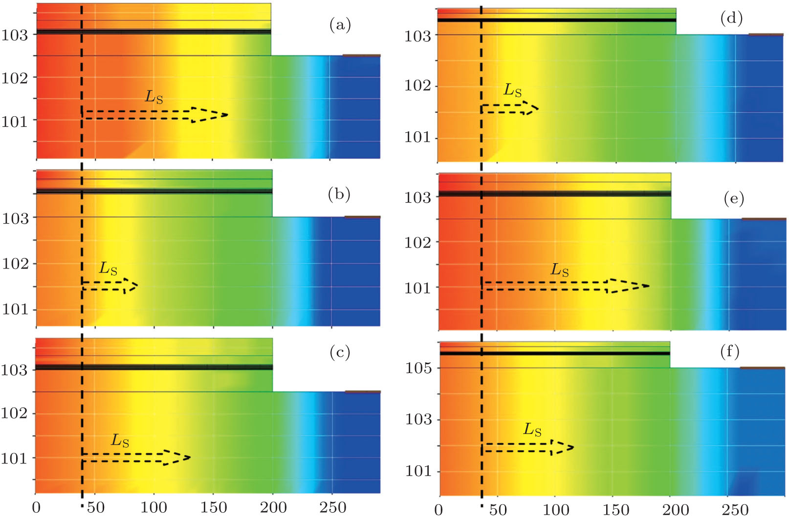
Two-dimensional distribution of current density. (a) Only double the thickness of the ITO layer (ρito = 3.5 × 10⁻⁶ Ω·m, tito = 400 nm). (b) Only double the resistivity of the ITO layer (ρito = 7.0 × 10⁻⁶ Ω·m, tito = 200 nm). (c) Double both the thickness and resistivity of the ITO layer (ρito = 7.0 × 10⁻⁶ Ω·m, tito = 400 nm). (d) Only double the thickness of the n-GaN layer (ρ = 9.09 × 10⁻⁴ Ω·m, t = 5 μm). (e) Only double the resistivity of the n-GaN layer (ρ =18.18 × 10⁻⁴ Ω·m, t = 2.5 μm). (f) Double both the thickness and resistivity of the n-GaN layer (ρ = 18.18 × 10⁻⁴ Ω·m, t = 5 μm). |

