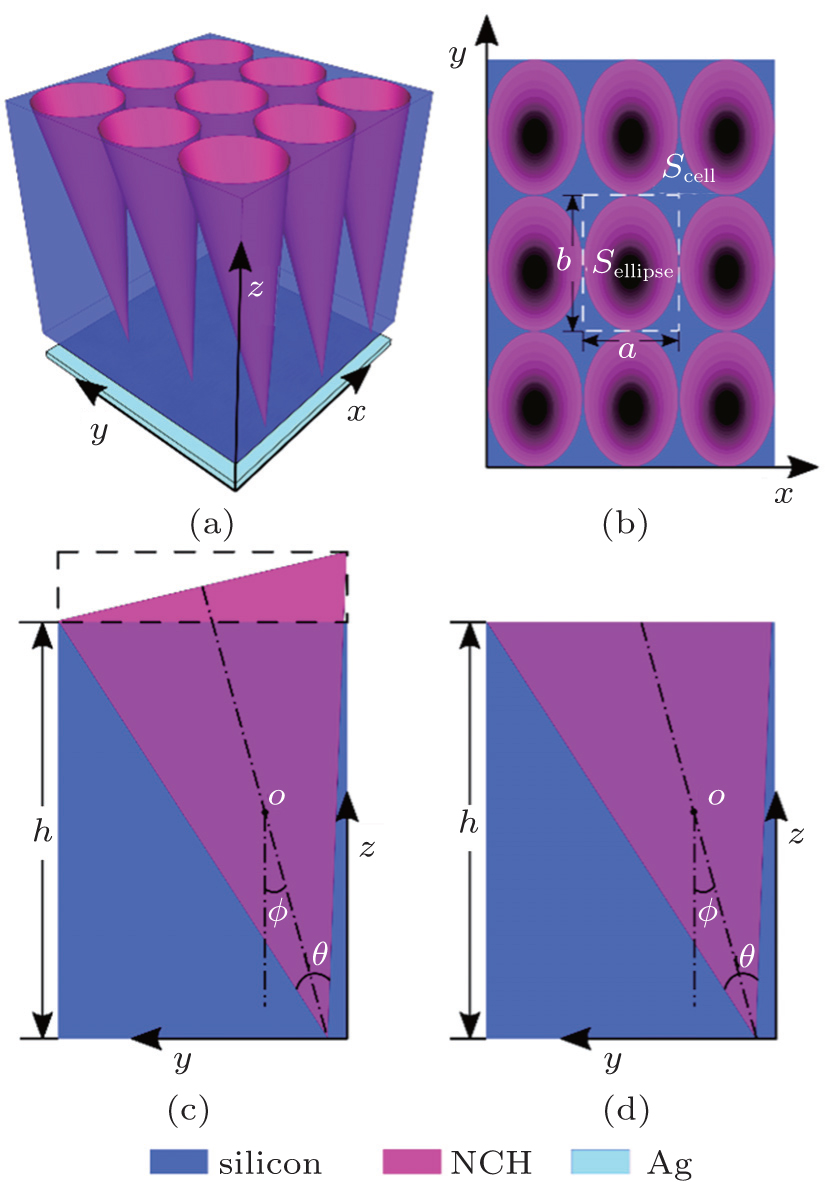
(a) Schematic diagram of the proposed slanted NCH array textured silicon thin film layer with an Ag back-reflector located under the bottom of it. (b) The top view of the slanted silicon NCH array. Sellipse represents the area of ellipse, while Scell represents the area of silicon unit cell surface. The filling factor FF = Sellipse/Scell. a and b are the lattice constants of the slanted NCH along the x and y directions, respectively. Panels (c) and (d) show the side views of the slanted silicon NCH before and after removing the excrescent part. θ and ϕ are the taper angle and tilt angle of the NCH, respectively. The black dashed line is the height of the NCH while O is the middle point of the height. h is the height of the silicon unit cell. |
 , Yang Fu-Hua