Scaling dependence of memory windows and different carrier charging behaviors in Si nanocrystal nonvolatile memory devices
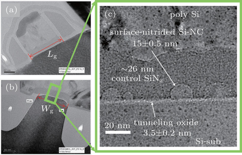
The cross-section TEM images of test key cell D along the (a) gate length and (b) width. (c) The high resolution cross-section TEM image of the Si-NC floating gate structure.

