A high-quality factor hybrid plasmonic nanocavity based on distributed Bragg reflectors
Tu Linlin1, Zhang Chi1, Huang Zhong1, Yau Jason1, 3, Zhan Peng1, 2, †, , Wang Zhenlin1, 2, ‡,
School of Physics and National Laboratory of Solid State Microstructures, Nanjing University, Nanjing 210093, China
Collaborative Innovation Center of Advanced Microstructures, Nanjing 210093, China
School of Physics, University of Western Australia, Perth WA 6009, Australia


† Corresponding author. E-mail: zhanpeng@nju.edu.cn

‡ Corresponding author. E-mail: zlwang@nju.edu.cn

Project supported by the National Key Basic Research Special Foundation of China (Grant Nos. 2012CB921501 and 2013CB632703) and the National Natural Science Foundation of China (Grant Nos. 11274160, 91221206, and 51271092).

Abstract
Abstract

Herein, we propose a high-quality (Q) factor hybrid plasmonic nanocavity based on distributed Bragg reflectors (DBRs) with low propagation loss and extremely strong mode confinement. This hybrid plasmonic nanocavity is composed of a high-index cylindrical nanowire separated from a metal surface possessing shallow DBRs gratings by a sufficiently thin low-index dielectric layer. The hybrid plasmonic nanocavity possesses advantages such as a high Purcell factor (Fp) of up to nearly 20000 and a gain threshold approaching 266 cm−1 at 1550 nm, promising a greater potential in deep sub-wavelength lasing applications.

1. Introduction

Optical resonant cavities have attracted a great deal of attention because of their ability to manipulate optical energy in small volume and to consequently tailor light-matter interactions. This ability is of great importance, for it facilitates useful practical applications in designing optical filters, switches, low-threshold lasers, brighter single-photon sources, and so on.[19] Moreover, both confining the light in high-Q cavities to increase the lifetime of the optical excitation and reducing the effective mode volume (Veff) are crucial in the designs of the optical resonant cavities.[10]

Surface plasmon (SP) is the collective electron charge oscillations that exist at the interface between the metal and dielectric media. It is capable of producing highly enhanced optical fields below the diffraction limit, which yields great potential to confine and manipulate light at sub-wavelength scale with a reduced Veff.[11] As a result, recently, plasmonic resonators have been presented widely in theory and experiment, including diverse metallic nanocavities making use of localized SP (LSP)[1215] and surface plasmon polaritons (SPPs).[10,16] However, the Q factors of LSP resonators are limited because of radiation and metallic losses. Although the SPPs resonators exhibit higher Q factors compared to LSP resonators, the former also suffer from huge propagation loss. In order to reduce propagation loss while offering tight mode confinement at sub-wavelength scale, a hybrid plasmonic waveguide comprised of a high-index dielectric nanowire separated from a silver surface by a nanoscale low-index dielectric gap was proposed,[17] which appears to be helpful in improving the Q factors of SPPs resonators. Subsequently, a plasmon laser[18] based on this kind of hybrid plasmonic waveguide was successfully demonstrated, and the feedback mechanism of this nanometer-scale plasmonic laser is based on a Fabry–Perot cavity provided by reflection of the nanowire end-facets. Taking into account the low reflection of the nanowire end-facets, we hope to further improve the Q factors of cavities by introducing high-reflectivity DBRs,[10,16] while maintaining a small mode volume.

In this letter, we design a hybrid plasmonic nanocavity based on DBRs, with an ultra-small mode volume and a high Q factor. As an example, Purcell factor of up to nearly 20000 and low gain threshold are achieved at 1550 nm, which are preferred to enable highly efficient nanocavity feedback for the potential applications such as deep sub-wavelength scale lasing.

2. Device model and numerical method

The proposed hybrid plasmonic nanocavity, as shown in Fig. 1(a), consists of a high-index GaAs nanowire separated from a Ag surface possessing shallow periodic gratings by a very thin low-index SiO2 dielectric layer. The background is also made out of SiO2 dielectric materials. The shallow periodic gratings serve as high-reflection DBRs, and two identical DBRs are placed along the direction of the GaAs nanowire with a selective distance between them to define a Fabry–Perot nanocavity, of which the length is L1. The lengths between the cavity edge and its adjacent DBRs are defined as L2, as shown in Fig. 1(a). The properties of this hybrid plasmonic nanocavity are investigated using COMSOL Multiphysics, a commercial finite-element-method-based software package. In our numerical simulations, the dielectric property of Ag is taken from Johnson & Christy[19] and the permittivities of GaAs and SiO2 are set to be 12.25 and 2.25.

Fig. 1. (a) Schematic diagram of the hybrid plasmonic nanocavity, which comprises a high-index semiconductor nanowire separated from a patterned metal substrate by a nanoscale low-index dielectric gap. (b) Dependence of the real part of the effective refractive indices on the incident wavelength. The insets are the normalized electric field distributions in the yz plane corresponding to the two grating sub-period regions.

By controlling the hybridization of the fundamental guided mode of the 100 nm radius GaAs nanowire and the SPPs of the dielectric–metal interface at the telecommunication wavelength 1550 nm, we can simultaneously make sure tight mode confinement and single-mode propagation, as the dielectric gap width between the nanowire and the upper metal plane is set to g1 = 2 nm. The depth of the grooves are set as h = 25 nm, in other words, g2 = g1 + h = 27 nm. The center wavelength of the stop band is related to the mode effective refractive indices. The mode effective refractive indices are calculated and displayed graphically in Fig. 1(b). It shows the real part of the effective refractive indices of the guided-mode propagating in the gap region between the GaAs cylinder and the metal surface with patterned grooves as a function of incident wavelength. Here, neff1 and neff2 are the effective refractive indices of the two-grating sub-period regions with gap widths of g1 = 2 nm and g2 = 27 nm, respectively. The normalized electric field intensity distributions of the hybrid plasmonic mode in the yz plane are shown in the insets of Fig. 1(b), corresponding to these two-gap widths, which clearly show that the hybrid plasmonic mode can be strongly confined in the gap region. In order to make sure the stop band is around 1550 nm, the grating period is designed to P = 400 nm and the width of the grooves are assumed as P/2 for simplicity.

3. Simulation results and discussion

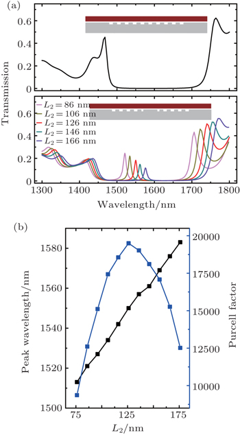
The optical properties of the hybrid plasmonic nanocavities are subsequently investigated. In order to evaluate the propagation performance of the DBR, the transmission of a DBR grating composed of 10 periods with periodicity P = 400 nm is simulated as plotted in the upper panel of Fig. 2(a). The incoming hybrid plasmonic mode tightly confined in the gap region between the patterned metal surface and nano-cylinder is reflected with > 99% efficiency, thus forming a stop band with a bandwidth of 200 nm, ranging from 1500 nm to 1700 nm, which actually can be tuned by varying the grating period. A hybrid plasmonic nanocavity with length L1 = 770 nm can be constructed by placing two identical 5-period DBRs together for the defect state located around 1550 nm. The transmission spectra of the hybrid plasmonic nanocavities with different L2 (the lengths between the cavity and its adjacent DBRs) are presented in the bottom panel of Fig. 2(a), in which there exist sharp resonant peaks located inside the stop band, and as L2 increases, the resonant peaks red-shift obviously. In principle, a high-performance nanocavity can be scaled over a broad wavelength range for the target wavelength by optimizing the geometry of the nanostructure such as the parameters L1 and L2.

For example, when L2 = 126 nm, a hybrid plasmonic nanocavity with resonant wavelength at 1550 nm can be achieved. Here, we use the ratio of the center wavelength of the resonant peak (λc) and its full width at half maximum (FWHM) to define the Q factor of this hybrid plasmonic cavity mode (Q = λc/FWHM). In this case, the transmittance of sharp resonant is 18.3% at λc = 1550 nm and the corresponding FWHM is 8.3 nm, which leads to a high Q factor of 187 owing to the low propagation loss. Since the transmission and FWHM of the resonant peak in the hybrid plasmonic nanocavity depend upon the period number (N) of the DBRs, as N increases, the FWHM reduces accordingly.[20,21] As an example, when the N of each DBR is 7 and 10, the FWHM reduces to about 5.3 and 4.6 nm, yielding higher Q factors of up to 292 and 337, respectively. However, as N increases, the decrease of transmittance of the resonant peak will strongly limit the detection and its further application.[20,21] On the other hand, the mode volume of the proposed nanocavity can be calculated by

where W(r) is the energy density, defined as

When L2 = 126 nm, an ultra-small mode volume of 3.04 × 10⁻²² m3 can be achieved for the hybrid plasmonic nanocavity with length L1 = 770 nm.

Fig. 2. (a) Transmission spectrum of a 10-period DBR (upper panel) and transmission spectra of hybrid plasmonic nanocavity composed of two 5-period DBRs with different L2 (bottom panel). Insets are the schematics of each structure. (b) Dependence of the wavelength of the resonant peak and Purcell factor on the length L2, varied from 76 nm to 176 nm at a step of 10 nm (L1 = 770 nm).

Based on an overall consideration of the effect of Q factor and Veff on the nanocavity, the Purcell factor is introduced to characterize the performance of the proposed nanocavity. Moreover, the Purcell factor is also a figure of merit to represent the ability of a cavity for spontaneous emission enhancement, which is described as[22]

where λ is the resonance wavelength, Q is the quality factor, Veff is the effective mode volume, and neff is the effective refractive index of the nanocavity. The wavelength of the resonant peak and Purcell factor as a function of L2, are both shown in Fig. 2(b). With the increase of L2 from 76 nm to 176 nm, the wavelength of the resonant peak shifts monotonically from 1513 nm to 1583 nm. It is noted that as L2 is 126 nm, owing to the achievable high Q factor and ultra-small mode volume, the Purcell factor reaches its maximum value of 19498, a fairly high value compared with that of the nanocavities mentioned before.[10,15,22]

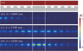
To illustrate the mode profile of the DBRs-based nanocavity clearly, the simulated normalized electric field intensity of the nanocavity in the xy plane at different wavelengths are plotted in Fig. 3. Here, for the proposed sample L2 = 126 nm, the hybrid plasmonic mode propagating characteristics for wavelengths at 1600 nm, 1740 nm, and 1550 nm are presented, which correspond to three typical wavelengths including inside the stop band, outside the stop band, and on resonance, due to the excitation of cavity mode, respectively. As shown in Fig. 3(b) at wavelength λ = 1600 nm, we observe that the light is reflected after a couple of periods inside the stop band. Moreover, the light propagates through the structure at wavelengths outside the stop band, as shown in Fig. 3(c), when the wavelength is at 1740 nm. Figure 3(d) shows that at λ = 1550 nm, the incident light couples and strongly resonances in the nanocavity.

Fig. 3. (a) Schematic diagram of the hybrid plasmonic nanocavity. Simulated normalized electric field intensity from the xy plane at the middle of the dielectric gap of hybrid plasmonic nanocavities at (b) λ = 1600 nm (inside the stop band), (c) λ = 1740 nm (outside the stopband), and (d) λ = 1550 nm (on resonance).

Due to the large Purcell factor, which represents the fine ability of the hybrid plasmonic nanocavity for spontaneous emission enhancement that was demonstrated in plasmonic nanoparticle antennas,[23] we also demonstrate the utility of the hybrid plasmonic nanocavity to control emission properties of dipole for the optimized L2 = 176 nm at wavelength of 1550 nm. Figure 4(a) shows simulated photoluminescence (PL) intensity spectra of x-, y-, and z-polarized dipole sources being placed at the center of our proposed DBRs-based hybrid plasmonic nanocavity. The PL intensity of z-polarized dipole source coupled to the cavity is much higher than that of x- and y-polarized one. This is because Ez is about three orders of magnitude higher than Ex and Ey at this point. The resonance peak of PL intensity spectrum of z-polarized dipole λ is 1550 nm, which corresponds well with transmission spectra of the cavity. Figures 4(b)4(d) show Ex, Ey, and Ez distributions in the yz plane of the cavity without dipole at λ = 1550 nm, respectively. The electric field distributions also reveal that Ez is much higher than Ex and Ey.

Considering the relatively high Q factor and ultra-small mode volume of the hybrid plasmonic nanocavity, we expect a low gain threshold for the lasing applications. To find out the gain threshold, a nanowire is chosen to be doped with optical gain material and we set the complex permittivity of the GaAs as . We then calculate the absorption efficiency for the hybrid plasmonic nanocavity with different gain coefficient . The zero absorption at a critical value, i.e., the gain threshold, means that loss in metal has been totally compensated by the gain in the nanowire. As a result, the gain threshold αth for the hybrid plasmonic nanocavity with L2 = 126 nm is calculated to be 266 cm−1, much smaller than that of the recently reported plasmonic lasing structures.[22,24]

Fig. 4. (a) Simulated PL intensity spectra for x- (black line), y- (blue line), and z-polarized (red line) dipole sources placed at the center of cavity with L2 = 126 nm. (b)–(d) Ex, Ey and Ez distributions in the yz plane of the cavity without dipole at the center of the cavity respectively.
4. Conclusion and perspectives

We design a hybrid plasmonic nanocavity with high Q factor and ultra-small mode volume based on the DBRs and the hybrid plasmonic waveguide. The characteristics of Purcell factor of up to nearly 20000 and low gain threshold approaching 266 cm−1 at the telecommunication wavelength 1550 nm provide efficient cavity feedback and high lasing efficiency. This result shows significant potential for sub-wavelength lasing applications and development of nanoscale integrated photonic circuits

Reference
1Noda SFujita MAsano T 2007 Nat. Photon 1 449
2Bianucci PWang XVeinot J GMeldrum A 2010 Opt. Express 18 8466
3Yanik M FFan SSoljacic M 2003 Appl. Phys. Lett. 83 2739
4Robinson J TChristina MLong CMichal L 2005 Phys. Rev. Lett. 95 143901
5Vahala K J 2003 Nature 424 839
6Wiersig JHentschel M 2006 Phys. Rev. 73 031802
7Akimov A VMukherjee AYu C LChang D EZibrov A SHemmer P RPark HLukin M 2007 Nature 450 402
8Kolesov RGrotz BBalasubramanian GStöhr R JNicolet A A LHemmer P RJelezko FWrachtrup J 2009 Nat. Phys. 5 470
9Chang D ESørensen A SHemmer P RLukin M D 2006 Phys. Rev. Lett. 97 053002
10de Leon N PShields B JYu C LEnglund D EAkimov A VLukin M DPark H 2012 Phys. Rev. Lett. 108 226803
11Gramotnev D KBozhevolnyi S I 2010 Nat. Photonics 4 83
12Hill M TOei Y SSmalbrugge BZhu Yde Vries Tvan Veldhoven P Jvan Otten FWMEijkemans T JTurkiewicz J Pde Waardt HGeluk E JKwon S HLee Y HNötzel RSmit M K 2007 Nat. Photonics 1 589
13Noginov M AZhu GBelgrave A MBakker RShalaev V MNarimanov E EStout SHerz ESuteewong TWiesner U 2009 Nature 460 1110
14Pan JChen ZChen JZhan PTang C JWang Z L 2012 Opt. Lett. 37 1181
15Xiao YLiu YLi BChen YLi YGong Q 2012 Phys. Rev. 85 031805
16Jiang HLiu CWang PZhang DLu YMing H 2013 Opt. Express 21 4752
17Oulton R FSorger V JGenov D APile D F PZhang X 2008 Nat. Photonics 2 496
18Oulton R FSorger V JZentgraf TMa R MGladden CDai LBartal GZhang X 2009 Nature 461 629
19Johnson P BChristy R W 1972 Phys. Rev. 6 4370
20Xu CHu TChen RPing YYang JJiang X 2013 J. Opt 15 105005
21Xiao JLiu JZheng ZBian YWang GLi S 2012 Phys. Status Solidi 209 1552
22Xiang CChan C KWang J 2014 Sci. Rep. 4 3720
23Chen XAgio MSandoghdar V 2012 Phys. Rev. Lett. 108 233001
24Li ZPiao RZhao JMeng XTong K 2015 Chin. Phys. 24 077303