Effect of NO annealing on charge traps in oxide insulator and transition layer for 4H-SiC metal–oxide–semiconductor devices
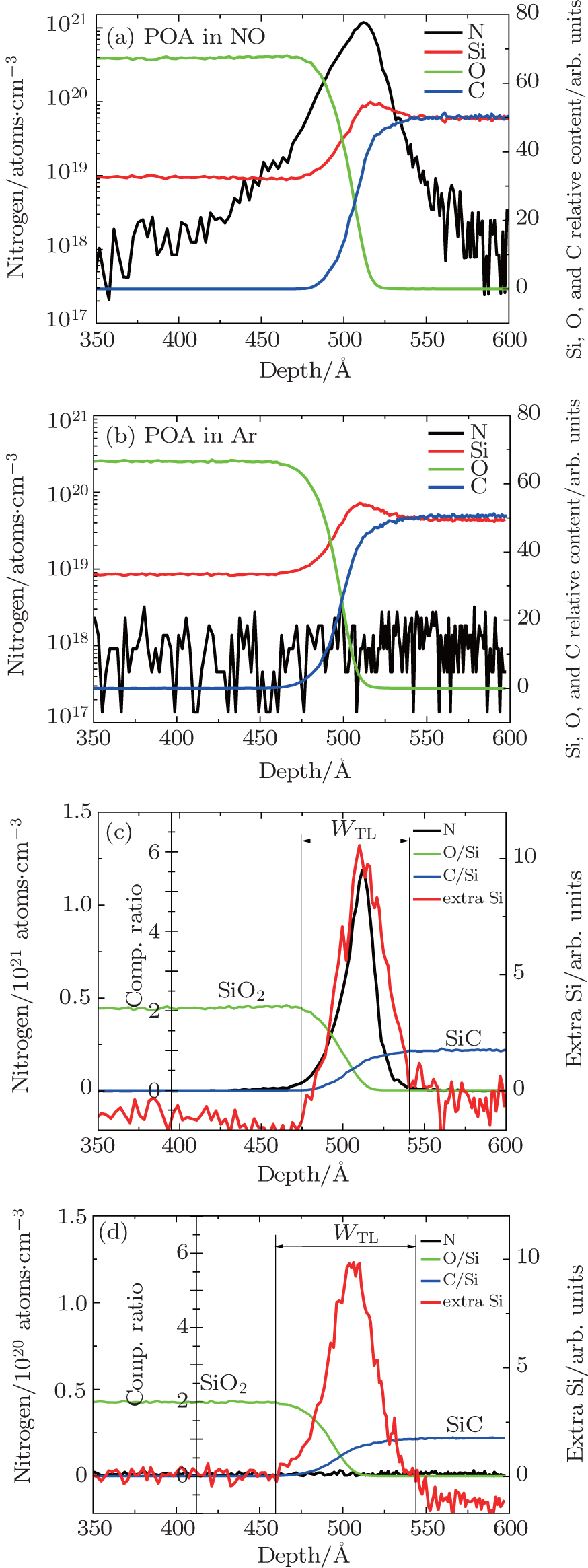
SIMS profiles for the (a) NO and (b) Ar annealed samples. Transition layer width extracted from O/Si and C/Si composition ratio curves and the excess Si relative content with (c) NO and (d) Ar annealing versus oxide thickness.

