† Corresponding author. E-mail:
‡ Corresponding author. E-mail:
Project supported by the National Natural Science Foundation of China (Grant Nos. 11374312, 51401230, and 51522105) and the Fund for Ningbo Municipal Science and Technology Innovation Team, China (Grant No. 2015B11001).
Free-standing antiferroelectric Pb(Zr0.95Ti0.05)O3 (PZT(95/5)) thin film is fabricated on 200-nm-thick Pt foil by using pulsed laser deposition. X-ray diffraction patterns indicate that free-standing PZT(95/5) film possesses an a-axis preferred orientation. The critical electric field for the 300-nm-thick free-standing PZT(95/5) film transiting from antiferroelectric to ferroelectric phases is increased to 770 kV/cm, but its saturation polarization remains almost unchanged as compared with that of the substrate-clamped PZT(95/5) film. The energy storage density and energy efficiency of the substrate-clamped PZT(95/5) film are 6.49 J/cm3 and 54.5%, respectively. In contrast, after removing the substrate, the energy storage density and energy efficiency of the free-standing PZT(95/5) film are enhanced up to 17.45 J/cm3 and 67.9%, respectively.
With the development of electronic devices towards miniaturization and light weight, electrical capacitors with high recoverable energy storage density and utilization are eagerly desired.[1–3] Currently, commercial high-power capacitors with energy density about 2.0 J/cm3 are mostly made of linear dielectric polymer materials with low dielectric constant, e.g., polypropylene, polyethylene terephthalate, and polyphenylene sulfide, because of their high dielectric breakdown strengths.[2] Recently, antiferroelectric materials, in which dipole moments are alternatively aligned in the opposite directions, resulting in the zero net polarization, have become the promising candidates for application in high energy storage due to an electric field forced phase transition from antiferroelectric into the ferroelectric states. Compared with the commercial capacitor, the electrical capacitor made of antiferroelectric material may achieve a higher energy density (more than 10.0 J/cm3)[4,5] and fast discharge speed (less than 20 ns).[6] Among various antiferroelectric materials, PbZrO3 based antiferroelectric materials have received extensive attention, owing to their possible energy storage densities as high as 50 J/cm3.[7] A lot of effort has been made to realize the theoretical prediction of energy storage density in the PbZrO3 related antiferroelectric material by doping elements,[8,9] local field engineering[10] or changing electrode material.[11,12] For example, Parui and Krupanidhi obtained a remarkable energy storage density of 14.9 J/cm3 at 600 kV/cm in La-doped PbZrO3 thin film.[8] Sa et al., reported a recoverable energy density as high as 17.4 J/cm3 in the α-Fe2O3 nanoparticles doped PbZrO3 thin film at 600 kV/cm.[10] Ge et al. found that the energy storage density and the energy efficiency of Pb0.97La0.02(Zr0.95Ti0.05)O3 film can be, respectively, enhanced to 14.8 J/cm3 at 1 MV/cm and 66% by using oxide metal LaNiO3 as top electrodes instead of Pt.[11]
On the other hand, the antiferroelectric-to-ferroelectric phase transition occurring in the antiferroelectric material is usually accompanied by a large volume change.[13] An external strain/stress can also effectively change the critical field of phase transition. Many researchers have investigated the influences of applied strain/stress on properties of the ferroelectric films.[14–18] However, only a few works have systematically studied this issue in antiferroelectric bulk or films.[19–21] Tan et al. found that the critical electric fields, i.e., EAF for the antiferroelectric-to-ferroelectric phase transition and EFA for the reverse transition, are shifted to high values by exerting the uniaxial or radial compressive stresses on the ceramic composition of Pb0.99Nb0.02[(Zr0.57Sn0.43)0.94Ti0.06]0.98O3,[20] which leads to the increase of energy storage density in the antiferroelectric capacitor.[22] Ayyub et al. found that PbZrO3 film presents ferroelectricity when its thickness is below 400 nm and show antiferroelectric behavior for the thickness above 550 nm due to the internal stresses caused by the substrate-clamping effect and their relaxation with thickness, which may result in the different energy storage densities and efficiencies for PbZrO3 films at various thicknesses.[19] After removing the stress by the substrate clamping, the energy storage properties of freestanding film may be changed. So far, a lot of freestanding ferroelectric films have been prepared by different methods.[23–25] In this paper, we fabricated antiferroelectric Pb(Zr0.95Ti0.05)O3(PZT(95/5)) films on both Pt foils and platinized Si substrates by using pulsed laser deposition. In comparison with those of the substrate-clamped reference sample (C-PZT(95/5)), the EAF and EFA of freestanding film (F-PZT(95/5)) are remarkably enhanced while its saturation polarization is slightly reduced. As a result, the energy storage density and the energy storage efficiency of the F-PZT(95/5) film are both significantly enhanced.
In our experiment, 200-nm-thick Pt foils, which were used as both the flexible substrates and the bottom electrodes, were obtained by etching platinized Si wafers (Pt(200 nm)/Ti(50 nm)/SiO2(500 nm)/Si) in 10 wt% HF solutions for 4 h. Due to the dissolution of the Ti layer and SiO2 layer in HF solutions, the thin Pt foils were detached from the wafers. The Pt foil was then transferred to a thermal oxide silicon wafer. The detailed procedures for preparing Pt foils were described in our previous publication.[17] The 300-nm-thick antiferroelectric Pb(Zr0.95Ti0.05)O3 films were grown on the Pt foils by pulsed laser deposition at 560 °C and 10-Pa oxygen pressure, with a KrF excimer laser (248 nm, Coherent Inc.) running at a repetition rate of 5 Hz and an energy density of 2.3 J/cm2. In order to characterize the electrical behaviors of antiferroelectric film, an array of circular Cu top electrodes (100 nm in thickness and 100 μm in diameter) was deposited on a PZT(95/5) layer with a metal shadow mask by e-beam evaporation. For comparison, 300-nm-thick C-PZT(95/5) film grown on platinized Si substrate was also prepared using the same parameters. The crystalline structures were characterized by an x-ray diffractometer (D8 Advance, Bruker) with Cu Kα radiation. The ferroelectric properties of F-PZT(95/5) and C-PZT(95/5) films were measured by a standardized ferroelectric test system (Precision Premier II, Radiant Technologies). Direct current (DC) electric field dependence of dielectric properties of the antiferroelectric films were measured by using a Keithley 4200 parameter analyzer.
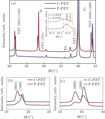
Figure
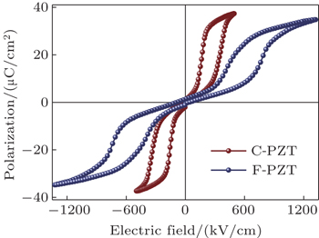
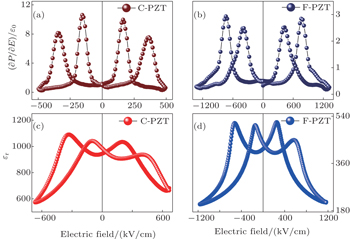
Such a change in structure of PZT(95/5) thin film should have a significant influence on its electrical properties. To bridge the structural and electrical properties in the antiferroelectric materials, polarization hysteresis loops of F-PZT(95/5) and C-PZT(95/5) films are measured at 10 kHz and at room temperature as shown in Fig.
As is well known, the electric displacement reflects the dipole orientation, while the dielectric constant indicates the motion of these dipoles. For a linear dielectric material, the dielectric constant can be related to the electric polarization as follows:

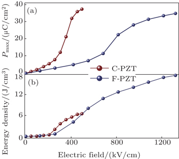
The energy storage density W of an antiferroelectric material can be obtained from the hysteresis P–E loop by using the relation

As shown in Table
| Table 1. Energy storage properties of both C-PZT(95/5) and F-PZT(95/5) membranes. . |
In this work, 300-nm-thick free-standing antiferroelectric PZT(95/5) film is successfully prepared on 200-nm-thick Pt foils by the pulsed laser deposition. The intensities of the (100) and (200) diffraction peaks of the F-PZT(95/5) film are increased after removing the substrate, indicating that F-PZT(95/5) film possesses an a-axis-preferred orientation. The antiferroelectric-to-ferroelectric electric field of the F-PZT(95/5) film increases up to 770 kV/cm compared with that of the substrate-clamped C-PZT(95/5) film. Therefore, the energy storage density and the energy storage efficiency are enhanced to 17.45 J/cm3 and 67.9%, respectively. Using the wafer bonding technology, the free-standing C-PZT(95/5) films can be integrated on any kind of flexible substrates, making them available for applications in flexible electrical devices such as capacitors and actuators.
| 1 | |
| 2 | |
| 3 | |
| 4 | |
| 5 | |
| 6 | |
| 7 | |
| 8 | |
| 9 | |
| 10 | |
| 11 | |
| 12 | |
| 13 | |
| 14 | |
| 15 | |
| 16 | |
| 17 | |
| 18 | |
| 19 | |
| 20 | |
| 21 | |
| 22 | |
| 23 | |
| 24 | |
| 25 | |
| 26 | |
| 27 | |
| 28 | |
| 29 | |
| 30 | |
| 31 | |
| 32 | |
| 33 | |
| 34 | |
| 35 | |
| 36 |


