† Corresponding author. E-mail:
Project supported by the National Natural Science Foundation of China (Grant No. 61177004).
We use Au@SiO2 nanoparticles (NPs) to systematically and comprehensively study the relationship between nanostructure and activity for surface-enhanced Raman scattering. Calculation simulation using the finite different time domain method verifies the experiment results and further reveals that the particle size and the distance between the NPs play vital roles in the surface-enhanced Raman scattering (SERS). Furthermore, in order to better simulate the real experiment, a Au@SiO2 nanosphere dimer is placed on the silicon substrate and Au substrate, separately. The simulation results show that the large EM field coupling is due to the “hot spots” transferred from the NP–NP gaps to NP–surface of metal gaps, meanwhile, more “hot spots” occur. We also find that the signal intensity strongly depends on the position of the probe molecule. This work provides a better understanding of EM field enhancement.
The Raman scattering from pyridine molecules adsorbed on a silver electrode surface can increase a million times or more as great as the signal from the free molecules. This is known as surface-enhanced Raman scattering (SERS).[1] Because it has high detection sensitivity, SERS technique has been widely applied to food safety,[2] electrochemistry,[3] and other fields.[4] As currently understood, SERS enhancement mode mainly includes electromagnetic (EM) coupling enhancement and chemical enhancement (CE).[5–8] The EM mechanism describes the enhanced local EM fields due to resonant excitation of plasma in the metallic nanostructure surface.[9,10] This purely physical effect is by far the most dominant contribution, with standard SERS enhancement factors (EFs) in a wide range of 103–1010. CE, only two–three orders of magnitude, is significantly smaller than the contribution of the EM coupling enhancement.[11] But how to validate the relationship between nanostructures and EM coupling is still a significant challenge in experiment.
Tip-enhanced Raman spectroscopy (TERS) was invented in 2000 — the pure Ag or Au or their coated atomic force microscope (AFM) tip acts as an antenna for both incident and Raman field.[12–14] If the substrate is metallic, the great EM field appears at the junction between the tip and substrate. This gap-mode can obtain much stronger Raman signal than normal SERS. It can even realize a single molecular detection limit for some resonant molecules.[15,16] However, there are some inherent defects. Firstly, for non-metallic surfaces there is no EM coupling between the tip and the substrate surface, the Raman signal of TERS is still too low to detect molecules. Secondly, the molecules in solution may be adsorbed on the tip and pollute the tip. Thirdly, the TERS instrument is too complicated and too expensive for practical application. In the market or human life, or other more practical applications, the material should be universal and available. This means that the signal should have good reproducibility. Meanwhile, the technique should be easily handled and cost-effective. The key advances made by shell-isolated nanoparticle-enhanced Raman spectroscopy (SHINERS) are a tremendous expansion of SERS versatility and much higher detection sensitivity than TERS.[17–19] In addition, SHIN can avoid the charge-transfer effect, therefore, the signal is more reliable and more stable. Precise control of the SiO2 shell thickness can bring convenience to study the EM coupling between the interparticle spacing.
The size, morphology, and interparticle spacing of the nanoparticles (NPs) are very important in the SERS, so a lot of research work mainly focused on using photoetching method to study the surface morphology, particle size and the interparticle spacing for SERS.[20,21] However, the high cost of sample prepared method hinders practical application. Therefore, we use the simple and feasible method through adjusting the shell thickness on the surface of NPs to study the particle size and interparticle spacing in the SERS here, in order to systematically understand the EM coupling effect relationship between the particle size and gap. Experimentally, Au@SiO2 NPs with 2-nm–3-nm shell thickness, and ca. 15-nm, 25-nm, 50-nm core sizes were prepared, respectively. Meanwhile, Au@SiO2 NPs with 25-nm core size, and ca. 3-nm, 15-nm, 35-nm, 50-nm shell thicknesses were prepared. A Au@SiO2 nanosphere dimer was chosen to simulate the experiment and calculate the EM field distribution by the finite different time domain (FDTD) method. Furthermore, in order to better simulate the real experiment, a Au@SiO2 nanosphere dimer was placed on the silicon substrate and Au substrate, separately. The simulation results show that the large EM field coupling is due to the “hot spots” transferred from the NP–NP gaps to NP–surface of metal gaps, meanwhile, more “hot spots” occur. The FDTD calculation results accord well with the experimental data. The findings in this work can guide us in designing the metallic nanostructures to obtain the strongest EM coupling enhancement.
Gold sol was prepared by the Frens method.[22] 100 ml of 0.01-wt% aqueous solution of HAuCl4 was placed in a round-bottom flask and heated to boiling under stirring. Next, 1 ml of 0.25-mM trisodium citrate solution was added quickly into the boiling solution, and the mixture was kept boiling gently for 30 min with continuous stirring. Then, the solution was cooled to the room temperature and put in a dark place before further use. By changing the amount of trisodium citrate which was added, to obtain different sizes of gold NPs, the sizes of 15 nm, 25 nm, and 50 nm of gold NPs were prepared.
For coating gold NPs with amorphous silica shells, two methods to prepare Au@SiO2 NPs were used. The first method according to classic Stober method:[23] 8-ml gold sol was dissolved in 20-ml isopropanol, and stirred for 3 min–5 min. Next, 0.5-ml aqueous ammonia was added rapidly, and then 5 μl of tetraethylorthosilicate (TEOS) was added, then stirred for 3 h. Different shell thickness can be obtained by controlling the reaction time and adding a certain amount of TEOS. With this method, we obtained Au NPs (∼ 25 nm) coated with SiO2 shell of thickness ca. 15 nm, 35 nm, and 50 nm, respectively.
The second method is presented by Li et al.,[17] 0.4 ml of 1-mM aqueous solution of (3-aminopropyl)trimethoxysilane (APTMS) was added to 30 ml of gold sol and stirred at 25 °C for 15 min. Subsequently, 3.2 ml of freshly prepared diluted sodium silicate solution (0.54 wt% of SiO2) adjusted with HCl to PH 9.6–PH 11 was added with stirring 3 min–5 min. Then, we placed the flask in a 90-°C water bath and stirred the contents for 10 min–60 min. After the reaction finished, the flask was placed in ice–water mixture to terminate the reaction quickly.
Au@SiO2 NPs monolayer film was prepared according to Li’s method.[24] 5 ml of cyclohexane was added in 15-ml Au@SiO2 NPs colloid. Then 4 ml of ethanol was added with stirring 3 min–5 min. Then, cyclohexane was removed with a glue dropper head. The Au@SiO2 NPs monolayer film was transferred onto gold film and silicon for further experiments. The scanning electron microscopy (SEM) images are shown in the Supporting Information (S1 and S2).
The gold film and silicon were purchased from German Tech Co., Ltd and Henghao Industrail, respectively. The average roughness of gold film was less than 3 nm. Prior to use, the gold film and silicon wafer were immersed in a mixture of concentrated sulfuric acid and hydrogen peroxide for 15 min, then rinsed by water and dried with nitrogen. The clean gold film and silicon were immersed in 10−6 mol/L R6G solution for 1 h–2 h and then rinsed with ethanol. After drying, the Au@SiO2 NPs monolayer film was transferred onto it.
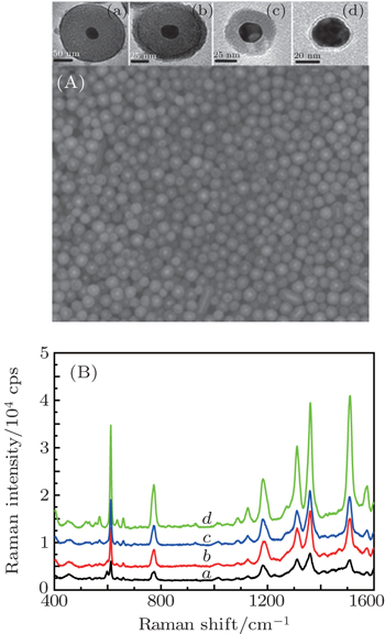
Experimentally, it is difficult to precisely control the distance between the Au NPs. In addition, the Raman signal will be distorted when the probe molecules directly contact bore Au NPs. Therefore, In order to analyze the effect of core size on the SERS signal, Au@SiO2 NPs with 2 nm–3 nm in shell thickness, and ca. 15-nm, 25-nm, and 50-nm core sizes are prepared, respectively, the transmission electron microscopy (TEM) images are shown in Fig.
In our experiment, the Au NPs with 25-nm average diameter have much better monodispersity. In order to verify the effect of the interparticle spacing on the same particle size, the Au@SiO2 NPs with core size 25 nm and different thicknesses are prepared as shown in Fig.
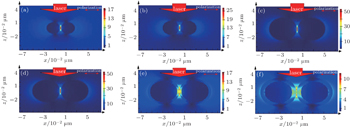
In the coupled NP system, an Au@SiO2 nanosphere dimer is chosen to simulate the above SERS experiment and calculate the EM field distribution by the finite different time domain (FDTD) method. The calculation results show that the particles’ size and the distance between the NPs play vital roles in the Raman signal enhancement. As shown in Figs.
Actually, very strong EM field is only observed in “hot spots” in junctions between two particles. As is well known, the maximum EM field is tightly confined near the NPs surface. Only the molecules which are absorbed on or very close to the gap can have a giant enhancement from SERS. The signal enhancement is determined by the NP size, the gap, and the position of the probe molecules in the “hot spots”. In addition, only the averaged surface enhancement factor (ASEF) can veritably and fully reflect the overall enhancement of the substrate. A simple calculation is offered to explain ASEF, only a few molecules (ca. 2%) in “hot spots” contribute to 98% of the total Raman signals, the average of all molecules Raman signal from the nanoparticle surface is still weak. How to obtain the strongest Raman signal and much more “hot spots” in the metallic nanostructures is still an enormous challenge in experiment.
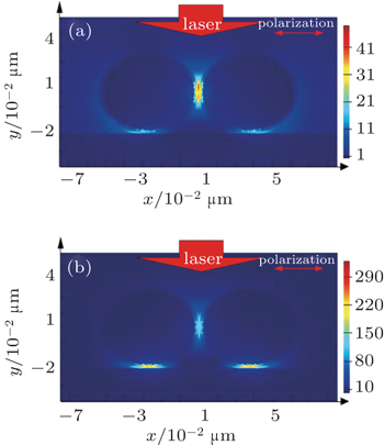
In practice, glass sheets and silicon wafers are widely used as the supports of metal NPs. The FDTD method is used to simulate the EM field distribution of the Au@SiO2 NPs on different substrates (parameters: diameter dAu = 50 nm, shell thickness = 2 nm, λ = 633 nm). As shown in Fig.
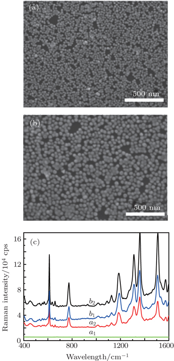
In order to verify the theoretical calculation and simulation accuracy, experimentally, the monolayer film of Au@SiO2 NPs of ca. 50-nm diameter is transferred on the Au film and silicon substrate after rinsing with ethanol. The scanning electron microscopic images are shown in Figs.
In order to obtain the strongest electric field and much more “hot spots” in the metallic nanostructures, the FDTD method is used to simulate and calculate the EM field distribution in Au@SiO2 NPs dimer on the different substrates. The calculation results show that on the silicon substrate, the bigger the particle size, the narrower the gap is and the stronger the EM field coupling intensity is. In addition, if the dimers disperse on the Au substrate, the signal comes from the gap region between the Au@SiO2 NPs and the substrate instead of the gap between the dimers, and it has much more “hot spots” and high EFs. Experimentally, Au@SiO2 NPs are prepared by using two methods, and Raman enhancements on different substrates are investigated. The FDTD calculation results fit well with the experimental data. Furthermore, we find that the signal intensity is determined not only by the NP size and the gap, but also by the position of the probe molecules in the “hot spots”. The findings in this work can guide us in designing the metallic nanostructures to obtain a strongest field enhancement.
| 1 | |
| 2 | |
| 3 | |
| 4 | |
| 5 | |
| 6 | |
| 7 | |
| 8 | |
| 9 | |
| 10 | |
| 11 | |
| 12 | |
| 13 | |
| 14 | |
| 15 | |
| 16 | |
| 17 | |
| 18 | |
| 19 | |
| 20 | |
| 21 | |
| 22 | |
| 23 | |
| 24 |


