Electronic transport properties of silicon junctionless nanowire transistors fabricated by femtosecond laser direct writing
Ma Liu-Hong, Han Wei-Hua†,  , Wang Hao, Lyu Qi-feng, Zhang Wang, Yang Xiang, Yang Fu-Hua‡,
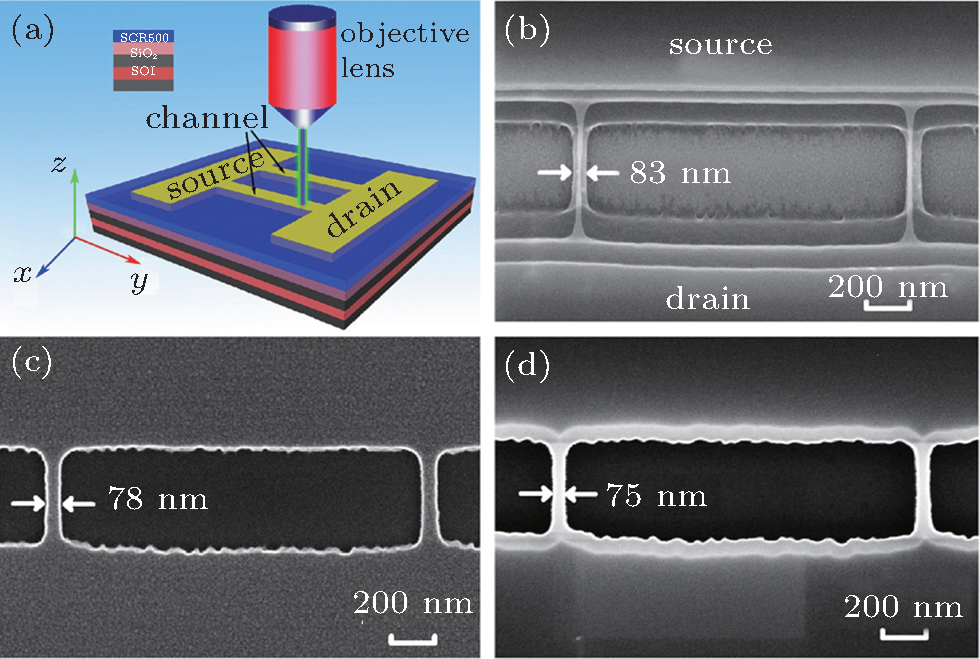
, Wang Hao, Lyu Qi-feng, Zhang Wang, Yang Xiang, Yang Fu-Hua‡, (a) Schematic diagram of femtosecond laser process, (b) SEM image of the photoresist patterns, (c) SiO2 patterns, and (d) silicon patterns after removing SiO2 mask of the twin-channel JNT.