All-dielectric frequency selective surface design based on dielectric resonator
Wang Zheng-Bin1, 2, †, , Gao Chao1, Li Bo1, 2, Wu Zhi-Hang1, Zhang Hua-Mei1, Zhang Ye-Rong1
School of Electronic Science and Engineering, Nanjing University of Posts and Telecommunications, Nanjing 210023, China
State Key Laboratory of Millimeter Waves, Nanjing 210096, China


† Corresponding author. E-mail: wangzb@njupt.edu.cn

Project supported by the National Natural Science Foundation of China (Grant Nos. 61201030, 61372045, 61472045, and 61401229), the Science and Technology Project of Jiangsu Province, China (Grant No. BE2015002), the Open Research Program of the State Key Laboratory of Millimeter Waves, China (Grant Nos. K201616 and K201622), and the Nanjing University of Posts and Telecommunications Scientific Foundation, China (Grant No. NY214148).

Abstract
Abstract

In this work, we propose an all-dielectric frequency selective surface (FSS) composed of periodically placed high-permittivity dielectric resonators and a three-dimensional (3D) printed supporter. Mie resonances in the dielectric resonators offer strong electric and magnetic dipoles, quadrupoles, and higher order terms. The re-radiated electric and magnetic fields by these multipoles interact with the incident fields, which leads to total reflection or total transmission in some special frequency bands. The measured results of the fabricated FSS demonstrate a stopband fractional bandwidth (FBW) of 22.2%, which is consistent with the simulated result.

PACS: 81.05.Xj;41.20.Jb
1. Introduction

Frequency selective surfaces (FSSs) are planar structures composed of a periodic array of unit cells that filter electromagnetic (EM) waves impinging on the surfaces.[1] They have been widely used in stealth technology, electromagnetic countermeasure, and communication systems.[1,2] Typical FSSs are composed of metallic grids or dipole arrays, which exploit the strong interactions between EM waves and metals. However, metals are problematic at very high incident power. For example, strong currents in the conductors will incur severe heating due to ohmic losses; arcing will occur at field concentration points.[3] Besides, metal materials are not quite favorable for high-temperature resistance and corrosion-resistant requirements. In Ref. [4], Li and Behdad cleverly reduced the amplitude of the local electric field by miniaturizing the metal FSS element and alternating layers of dielectric and metal grids to separate the capacitive and inductive layers. However, consider that dielectrics exhibit a much weaker interaction with the field than metals do, then all-dielectric FSSs will turn more alternative.

Recently, Barton et al.[5] developed an all-dielectric FSS (ADFSS) based on guided-mode resonance (GMR), which extends the fractional bandwidth of conventional GMR devices from 1% to 16%, and could survive with no damage at a high pulsed microwave power of 1.7 GW/m2. Barton et al.[6] designed another novel ADFSS by using genetic algorithms and fast Fourier transforms to generate random geometries, which exhibits a larger fractional bandwidth. Each of the two designs has a total height about λ0/3(λ0 is the center wavelength of the operating EM wave). In the optical region, subwavelength dielectric granules that possess strong Mie resonances are often used to fabricate double-negative metamaterials,[7] single-negative metasurfaces,[8,9] and impedance matched zero-index metamaterials.[10] Recently, a single-negative all-dielectric metamaterial, which is comprised of a single layer of cylindrical silicon resonators on a silicon-on-insulator substrate, has been experimentally proved to possess broadband perfect reflection in the infrared region.[8]

In this work, we exploit the method of all-dielectric metamaterials to develop all-dielectric FSSs, where high-permittivity dielectric resonators (DRs) are periodically placed in a three-dimensional (3D) printed supporter. The fabricated ADFSS exhibits a stop-band fractional bandwidth of 22.2% with a total height of less than λ0/6. Owing to the thinner thickness, the field of view (FOV) is also greatly improved. The symmetric structure of the device makes it insensitive to polarization.

2. Theoretical analysis of dielectric resonator characteristics

According to Mie scattering theory,[11,12] when a plane wave impinges on a single electrically-small dielectric particle (with the relative permittivity εr = n2) located in a background material with dielectric constant εb and permeability μb, the field distribution of the scattered wave can be decomposed into multipolar components with plane wave expansions. The scattered field Es induced by a particle can in general be expressed as an infinite series in the vector spherical harmonics Nemn and Momn (where the subscripts e and o represent even and odd, respectively), the so-called EM normal mode of the electrically-small particle is weighted by appropriate coefficients amn and bmn, and expressed as[1214]

where the index n indicates the degree of the multipole (1 = dipole, 2 = quadrupole, 3 = octupole, etc.), and m indicates the possible orientation of the multipole. When these subwavelength dielectric particles are placed as a two-dimensional array, the scattered fields by all the particles will be superposed, which may lead to some special propagation properties. From the viewpoint of effective-medium theory for metamaterials, such an array can be described with frequency-dependent effective permittivity (εeff) and permeability (μeff),[15] which depends on the number of small particles per unit volume (N) and the coefficients amn and bmn in Eq. (1). Through appropriately choosing amn and bmn, we can obtain minus εeff or minus μeff in the vicinity of an electric or a magnetic resonance. When the electric and magnetic resonances are spectrally isolated, the real parts of the permittivity and permeability of the medium have opposite signs.[8] In this case, EM waves cannot pass through the medium. On the contrary, when electric and magnetic resonances occur at the same frequency point, the structure exhibits double-negative properties and a transmission pole will appear.

As is well known, high-permittivity dielectric cylinders can be regarded as magnetic-wall structures approximately. When EM waves enter into a DR, they will be reflected between the interfaces of the dielectric and free space continuously, which results in many resonant modes, including transverse electric (TE) modes, transverse magnetic (TM) modes, and hybrid electromagnetic (HEM) modes. For such a cavity, wave functions which are TE and TM with respect to the z direction can be written as[16]

where a and h are the radius and height of the DR, respectively, Jn is the Bessel function of the first kind, with Jn (Xnp) = 0, , n = 1,2,3, …, p = 1,2,3, …, m = 1,2,3, …. From the separation equation , the resonant frequency of the npm mode can be written as

The total far field scattered by a subwavelength DR can be decomposed into multipolar components, such as dipoles, quadrupoles, and so on. In most cases, higher-order terms are negligible. Then, the reradiate EM fields by these low-order multipoles interact with the applied field and lead to the overall frequency response.

3. Experimental results

In the work presented here, high-permittivity dielectric cylinders are used as the resonators due to their amenabilities to top-down fabrication techniques. For cylinder resonators, the position of the electric or magnetic dipole mode is a function of the aspect ratio h/D, where h and D are the height and diameter of the cylinder, respectively. It has been proved that the spectral separation of the electric and magnetic resonant modes approaches to the largest spacing as h/D ∼ 1.0, which is necessary for the design of broadband reflector.[8]

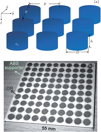
Figure 1(a) shows a prototype of the all-dielectric FSS, which is composed of an array of ceramic ((Zr, Sn)TiO4) cylinders. The device is designed to work in the Ku-band (12 GHz–18 GHz). The relative permittivity and loss tangent of the dielectric are εr = 38, tan δ ≈ 3 × 10⁻⁴, respectively. The height and diameter of the cylinders are h = 3.5 mm (∼ 0.16λ0, λ0 is the free-space wavelength centered at 13.5 GHz) and D = 4 mm (∼ 0.16λ0), respectively. The subwavelength period of the array is P = 5.5 mm (∼ 0.25λ0). In order to conveniently hold these DRs, a supporter is fabricated with a three-dimensional (3D) printer (Makerbot Replicator). The printing material is an acrylonitrile butadiene styrene (ABS) plastic with the relative permittivity εs = 2.6, which is much smaller than that of the DR. Simulation results (not shown here) have proved that the presence of the ABS has little influence on EM resonances. Figure 1(b) shows the fabricated all-dielectric FSS, which is an array of 10 × 10 unit cells. The whole dimension is 55 mm × 55 mm (∼ 2.5λ0 × 2.5λ0).

Fig. 1. (a) Schematic of the all-dielectric FSS with a center frequency of 13.5 GHz. The dimensions of the array of (Zr, Sn)TiO4 DRs are h = 3.5 mm, D = 4 mm, and P = 5.5 mm. (b) Final all-dielectric FSS under test.

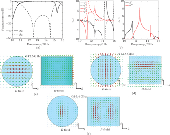
Firstly, we perform full-wave simulation with Computer Simulation Technology (CST) Microwave Studio,[17] where normally incident plane waves are assumed. Figure 2(a) shows the simulated results. The dashed line in this figure demonstrates two transmission zeros (at 12.5 GHz and 14.5 GHz) and one transmission pole (at 15.5 GHz). Then, the effective EM properties of the electrically-thin FSS are extracted from the simulated S-parameters[15,18] as shown in Fig. 2(b). From the figure we can see that the medium is single negative with ε′ < 0 and μ > 0 between 11.43 GHz and 14.47 GHz, and with ε′ > 0 and μ′ < 0 between 11.47 GHz and 15.32 GHz. This results in an extreme impedance mismatch with z′ = 0 across the bandwidth. From Fig. 2(b) we can also see that in the vicinity of the transmission pole (15.5 GHz), the medium is double negative, and the impedance is matched with the air (z′ ≈ 1)

Fig. 2. (a) The simulated transmission properties of the ADFSS. (b) Effective permittivity and permeability (left), and the retrieved z′ and n″ (right) of the DR-based FSS. (c)–(e) The electric and magnetic field distributions inside the DR at 12.5 GHz (c), 14.5 GHz (d), and 15.4 GHz (e) respectively.

In order to further explore the physical mechanism of the resonance, we obtain the time snapshots of the steady-state electric and magnetic field at the two transmission zeros and the transmission pole from the CST Microwave Studio. Figure 2(c) shows that at 12.5 GHz the E-field inside the DR exhibits a loop-shape distribution in the yz plane, while the H-field in the xy plane forms a magnetic dipole. Nevertheless, figure 2(d) shows that at 14.5 GHz the H-field in the xz plane exhibits a loop-shape distribution, while the E-field in the xy plane forms an electric dipole. Here, we should notice that both the magnetic dipole and the electric dipole are perpendicular to the propagation direction of the incident wave (z direction). For the transmission pole at 15.5 GHz, the field distributions in Fig. 2(e) show an electric dipole in the xy plane and a magnetic quadrupole in the xz plane. The magnetic quadrupole is parallel to the propagation direction of the incident wave (in the z direction).

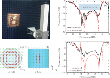
Then, the manufactured ADFSS is experimentally tested in our anechoic facility (shown in Fig. 3(a)) to verify the simulated transmission property. The illuminating broadband horn is placed 1.5 m (∼ 65λ0) away from the ADFSS to better approximate a plane wave. Another receiving horn antenna is placed 1.0 m behind the device to detect the transmitted power. For normally incident plane waves, the measured transmittance S21 through the ADFSS is shown in Fig. 3(b) (the black solid line), which coincides with the simulated results well. The −15 dB FBW approaches to 22.2%. To study the effective angle of incidence on this ADFSS, we swept the azimuthal angle from 0° to 30°, keeping the elevation angle fixed at 0°. Simulation results (not shown here) demonstrate that with the increase of the oblique incident angle, a resonance at 12 GHz becomes more and more strong. Figure 3(c) shows the simulated and measured results for 30° incidence. From the figure we can see that the −15 dB FBW has almost no change except for a sharp resonance at 12 GHz. Figure 3(d) further shows the electric and magnetic field distributions at the resonant frequency for 30° incident angle, where the electric field forms a loop, while the magnetic dipole is parallel to the propagation direction of the incident wave. How to suppress the sharp resonance deserves further exploration.

Fig. 3. (a) Experimental setup in the anechoic chamber. (b) Simulated and measured transmittance of the ADFSS under normal incidence and (c) at 30° incidence. (d) Electric and magnetic field distribution inside the DR at 12 GHz.
4. Conclusions

For high-power incident microwaves, FSSs composed of metallic unit cells are problematic. In this paper, we present a subwavelength-thick all-dielectric FSS composed of high-permittivity dielectric resonators and 3D printed supporter, which avoids all use of metals. Incident waves enter into the DRs and lead to electric and magnetic resonances, which can be decomposed into multipolar components. The reradiated fields by these multipoles interact with the applied field, leading to the overall frequency response. This fabricated all-dielectric FSS provides 15 dB of suppression over a 22.2% fractional bandwidth and large field of view except a very narrow frequency band at 12 GHz. This method will find a variety of potential applications in high-power microwave systems including radomes, electromagnetic protections, and more.

Reference
1Munk B A2000Frequency Selective Surfaces: Theory and DesignNew YorkWiley-Interscience
2Liu C HBehdad. N 2013 J. Appl. Phys. 113 064909
3Pugh S2010DTIC DocumentDefense Technical Information Center, Fort Belvoir, VA USA
4Li MBehdad N 2013 IEEE Trans. Antennas Propag. 61 677
5Barton J HGarcia C RBerry E AMay R GGray D TRumpf R C 2014 IEEE Trans. Antennas Propag. 62 3652
6Barton J HGarcia C RBerry E ASalas RRumpf R C 2015 IEEE Trans. Antennas Propag. 63 1032
7Peng LRan LChen HZhang HKong JGrzegorczyk T 2007 Phys. Rev. Lett. 98 157403
8Moitra PSlovick B AYu Z GKrishnamurthy SValentine J 2014 Appl. Phys. Lett. 104 171102
9Slovick BYu Z GBerding MKrishnamurthy S 2013 Phys. Rev. 88 165115
10Moitra PYang YAnderson ZKravchenko I IBriggs D PValentine J 2013 Nat. Photon. 7 791
11Bohren C FHuffman D R1983Absorption and Scattering of Light by Small ParticlesNew YorkWiley-Interscience
12Yang Y YQu S BWang J FZhao J BPeng BLi ZXia SXu Z 2011 Acta Phys. Sin. 60 074201 (in Chinese)
13Sihvola A1999IEEE Electromagnetic Waves Series 47The Institution of Electrical EngineersStevenage, Herts, UK
14Slovick B AYu Z GKrishnamurthy S 2014 Phys. Rev. 89 155118
15Hou Z LKong L BJin H BCao M SLi XQi X 2012 Chin. Phys. Lett. 29 017701
16Luk K MLeung K W2003Dielectric Resonator AntennasHertfordshireResearch Studies Press Ltd.
17“Computer Simulation Technology (CST) − – Microwave Studio”User's Manual42013http://www.cst.com.
18Szabo ZPark G HHedge RLi E P 2010 IEEE Trans. Microwave Theory Tech. 58 2646