

Broadband, polarization-insensitive, and wide-angle microwave absorber based on resistive film
Cite this Article
Bu Dan-Dan, Yue Chun-Sheng, Zhang Guang-Qiu, Hu Yong-Tao, Dong Sheng. Broadband, polarization-insensitive, and wide-angle microwave absorber based on resistive film. Chinese Physics B, 2016, 25(6): 067802 
Permissions
Broadband, polarization-insensitive, and wide-angle microwave absorber based on resistive film
† Corresponding author. E-mail:
Abstract
Abstract
A simple design of broadband metamaterial absorber (MA) based on resistive film is numerically presented in this paper. The unit cell of this absorber is composed of crossed rectangular rings-shaped resistive film, dielectric substrate, and continuous metal film. The simulated results indicate that the absorber obtains a 12.82-GHz-wide absorption from about 4.75 GHz to 17.57 GHz with absorptivity over 90% at normal incidence. Distribution of surface power loss density is illustrated to understand the intrinsic absorption mechanism of the structure. The proposed structure can work at wide polarization angles and wide angles of incidence for both transverse electric (TE) and transverse magnetic (TM) waves. Finally, the multi-reflection interference theory is involved to analyze and explain the broadband absorption mechanism at both normal and oblique incidence. Moreover, the polarization-insensitive feature is also investigated by using the interference model. It is seen that the simulated and calculated absorption rates agree fairly well with each other for the absorber.
PACS:
78.20.Ci;42.25.Bs;41.20.Jb
1. Introduction
The initial microwave absorber is Salisbury screen, which consists of the resistive layer surface, a quarter wavelength dielectric spacer, and the metal grounded plane.[1] As absorbing electromagnetic waves by thickness interference, Salisbury screen achieves the absorption of specific wavelengths of electromagnetic waves but obtains a narrow absorption band. Based on the absorbing mechanism of Salisbury screen, multilayer continuous resistive films and dielectric substrates arranged alternately with each other constitute Jaumann absorber.[2] In 2008, Landy et al. proposed the perfect metamaterial absorber (MA) first.[3] Subsequently, many MAs with new features were designed to achieve polarization-insensitive absorption[4–6] or wide-angle absorption.[7,8] However, most of these structures designed are based on strong electromagnetic resonance to effectively absorb the incident wave. Thus, the absorption bandwidths of these MAs are relatively narrow. In order to expand the absorption bandwidth, wideband MAs loaded lumped elements[9–11] have been proposed, but the cost is high and it is usually difficult to fabricate. Substituting the resistive pattern for the metallic structure, another class of MA is employed to implement broadband absorption,[12–14] which is easily processed and cost is low. For the theoretical analysis of absorbing properties of the MA, the generally accepted impedance matching principle can explain the absorption only qualitatively, while transmission line model[15,16] is only available in the case of normal incidence of electromagnetic waves with ignoring interaction between layers of absorbing structures. Compared with these two theoretical approaches, the interference theory[17–19] can not only quantitatively analyze the absorbing properties of MAs, but also quantitatively study the interaction between the internal metallic layers of the structures, meanwhile it is applicable to the complex structure under the oblique incidence condition. Previously, design and analysis of MAs using interference theory were focused on single-band and multi-band absorption.[20,21] Now, attention begins to shift to the study of wideband absorption of the MAs by using the interference theory. Chen et al. adopted first the interference model to explain the broadband absorption mechanism at both normal and oblique incidence.[14]
In this paper, we present a broadband, polarization-insensitive and wide-angle MA, which can be fabricated easily by traditional printed circuit board (PCB) technology and silk-screen printing.[14] The presented MA obtains wide frequency band absorption from 4.75 GHz to 17.57 GHz with absorption rate above 90%, and can achieve polarization-insensitive and wide-angle absorption for both TE and TM waves. The interference theory is used to explain the absorption mechanism at different angles of incidence and variable polarization angles.
2. Design and simulation
2.1. Absorption and distribution of power loss density
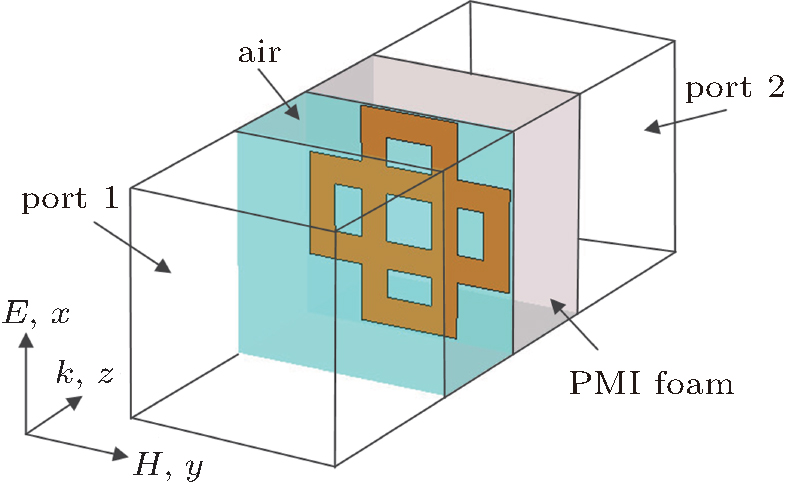
The proposed MA is designed and optimized by CST Microwave Studio based on the commercial finite difference time domain (FDTD) solver. The schematic diagram and geometric parameters of the absorber unit cell are shown in Fig.
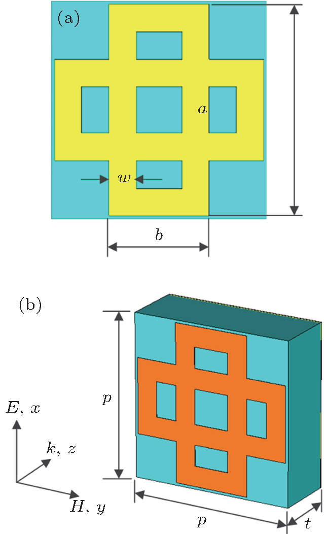 | Fig. 1. Schematic diagram with geometric parameters of the broadband absorber unit cell. (a) The front view and (b) the perspective view. |
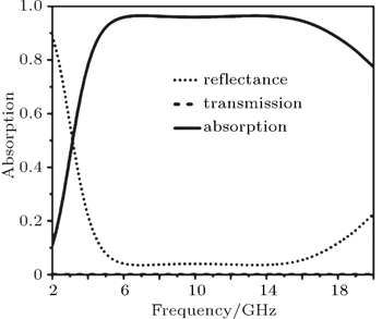
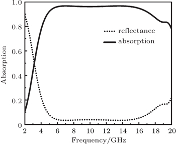
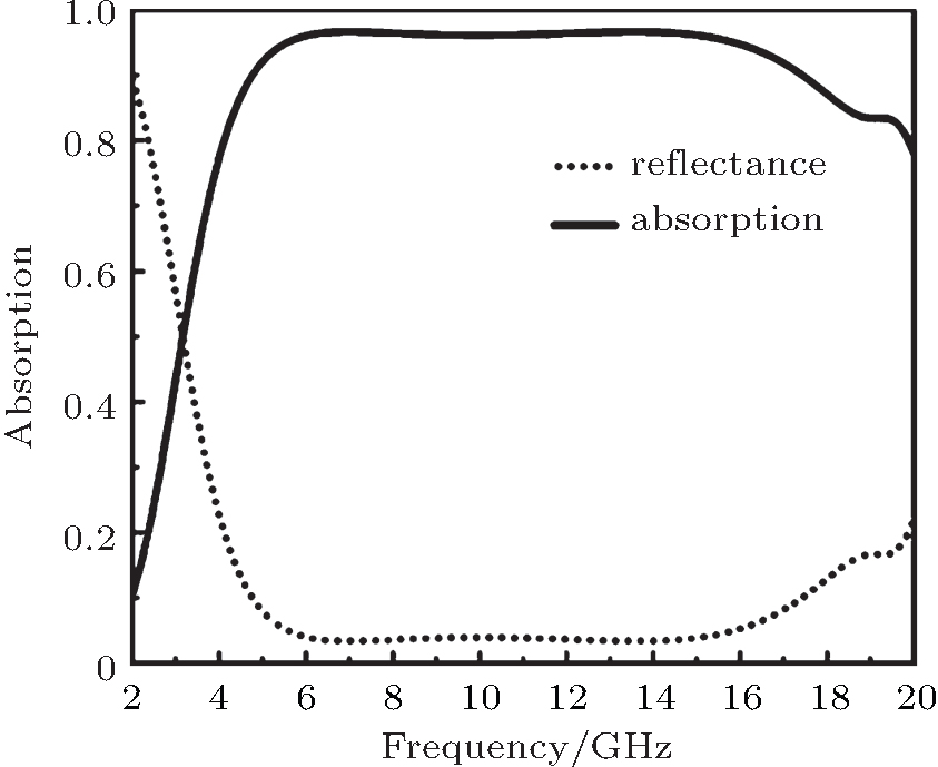
The simulated reflectance, transmission and absorption spectra of the MA are shown in Fig.
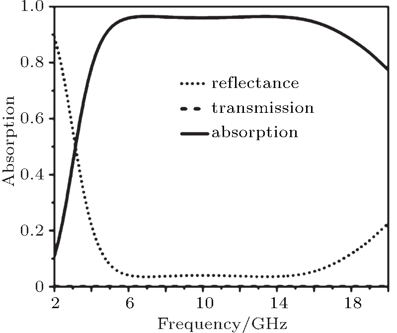 | Fig. 2. Simulated reflectance (short dot curve), transmission (short dash curve), and absorption spectra (solid curve) of the absorber each as a function of frequency. |
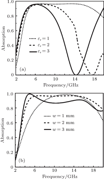
Considering the influences of substrate permittivity and width of the resistive film on the absorption of composite MA, we simulate the absorptivities of the MA with different substrate permittivities and widths of the resistive film as shown in Figs.
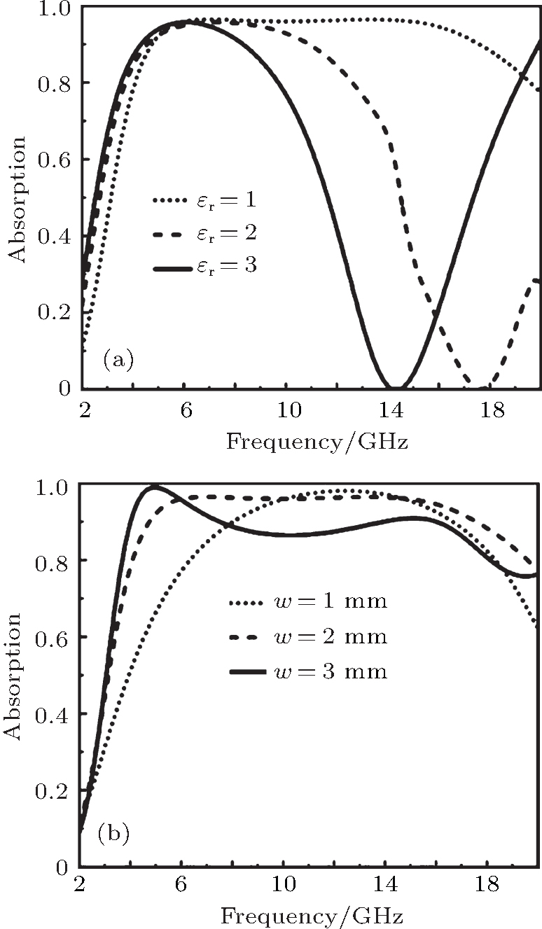 | Fig. 3. Simulated absorption spectra of the absorbers with (a) different substrate permittivities and (b) different widths of the resistive film. |
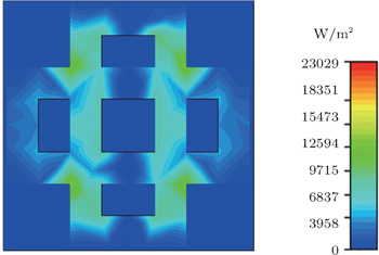
To gain an insight into the intrinsic absorption mechanism, the distribution of power loss density at the midpoint 11 GHz of the whole frequencies of interest is given in Fig.
 | Fig. 4. Distribution of surface power loss density at 11 GHz of the proposed absorber. |
2.2. Polarization-insensitive and wide-angle absorption
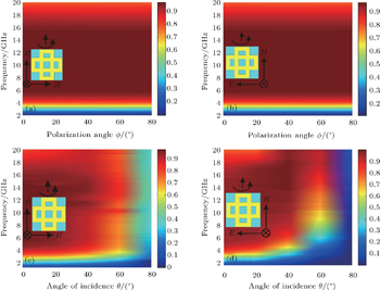
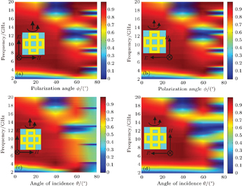
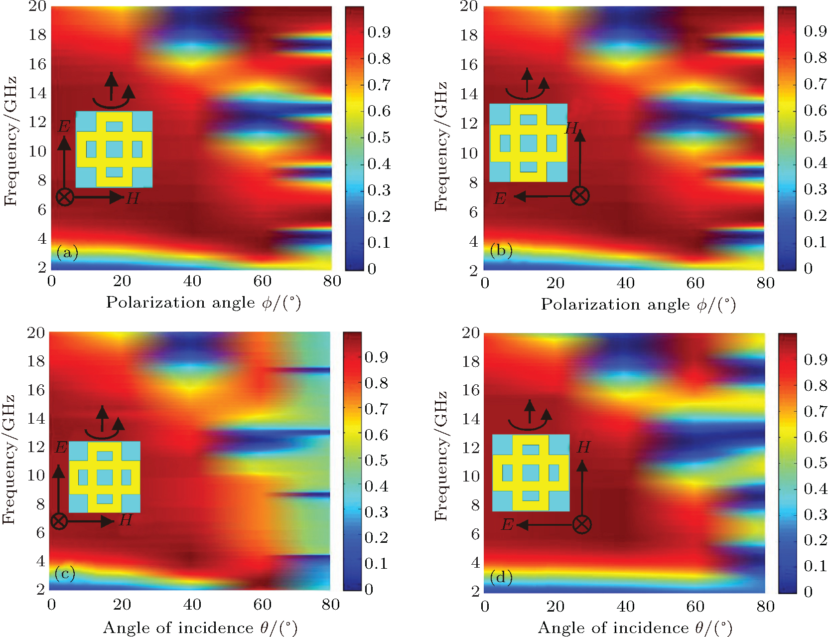
The polarization-insensitive feature is characterized by setting the polarization angles from 0° to 80° in steps of 20° at normal incidence. Figures
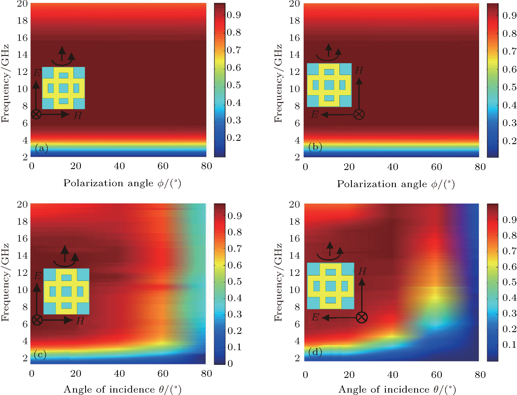 | Fig. 5. Simulated absorption rates of this MA at different polarization angles for (a) TE and (b) TM waves. Simulated absorption rates of this MA at different angles of incidence for (c) TE and (d) TM waves. |
Next, the performances of the proposed absorber at various incident angles are investigated. The simulated absorption rates at different angles of incidence for TE and TM waves are depicted in Figs.
3. Multi-reflection interference theory
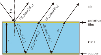
To reveal absorbing property of the absorber quantitatively, the interference theory is involved to analyze the broadband absorption mechanism. For an uncoupled absorber model, the near-field coupling between layers is negligible, while introducing compensation sheets can cover the near-field coupling between layers for strong coupling structure.[5,17,19,22,23] The interference model of the structure and relevant variables are shown in Fig.
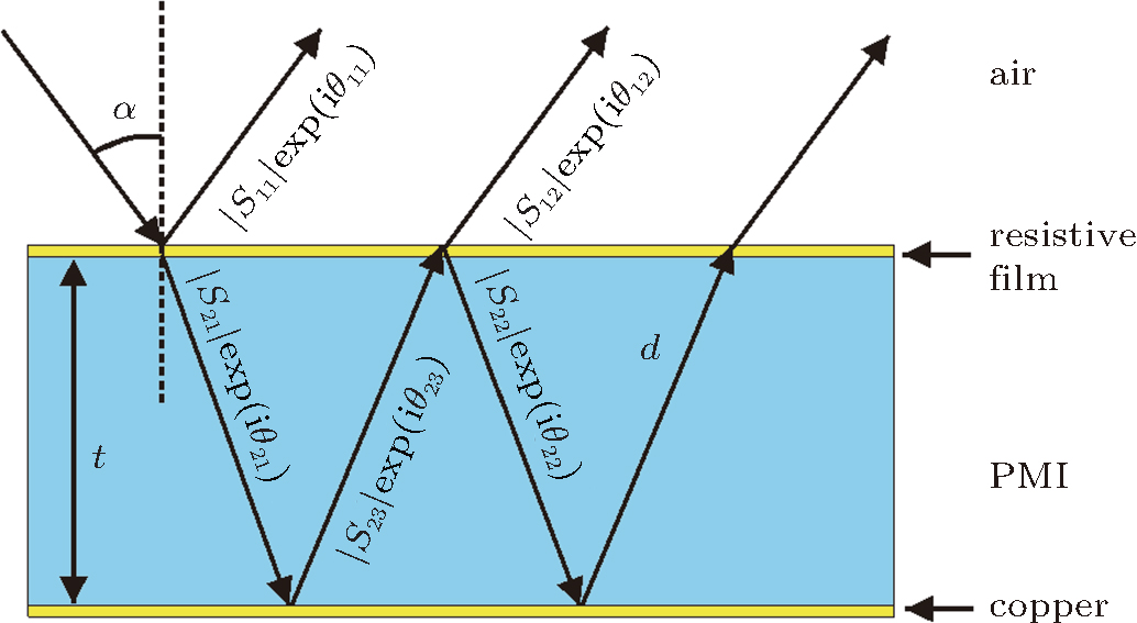 | Fig. 6. Interference model of the MA and relevant variables. |
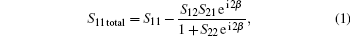
Therefore, according to the interference theory,[5,19] the superposition of multiple reflections at interface 1 (resistive film) from air back to air can reach the overall reflection, thus

As shown in Fig.
 | Fig. 7. Unit cell used to simulate S-parameters at interface 1. |
Figure
 | Fig. 8. Calculated reflection rate (short dot curve) and absorptivity (solid curve) by using the interference model. |
Additionally, the absorption rates of the proposed absorber at oblique incidence and variable polarization angles are also investigated by using the interference theory. Figures
 | Fig. 9. Calculated absorptivities each as a function of frequency and polarization angle for (a) TE and (b) TM waves. Calculated absorptovities each as a function of frequency and angle of incidence for (c) TE and (d) TM waves. |
The calculated absorption rates of the structure by using the interference model at different angles of incidence for TE and TM modes are shown in Figs.
4. Conclusions
In this work, we proposed a broadband, polarization-insensitive, and wide-angle MA based on resistive film, which exhibits absorption frequency band ranging from 4.75 GHz to 17.57 GHz with absorptivity above 90% at normal incidence. Distribution of surface power loss density indicates that the resistive film mainly supplies the broadband high absorption due to the ohmic loss. The MA can achieve polarization-insensitive absorption at the normal incidence and operate well at different angles of incidence for both TE and TM waves. The multi-reflection interference theory is adopted to quantitatively analyze the absorptions of the designed structure at different incidence angles and variable polarization angles for both TE and TM modes. Theoretical calculation and simulation results agree fairly well with each other at wide angles of incidence and wide polarization angles. Importantly, the proposed MA is also geometrically scalable. Therefore, our results are not limited to gigahertz frequencies and may be used in other parts of the electromagnetic spectrum. The designed MA has great promise for stealth technology and other relevant applications because of its broadband absorption and easy fabrication.
Reference
| 1 | |
| 2 | |
| 3 | |
| 4 | |
| 5 | |
| 6 | |
| 7 | |
| 8 | |
| 9 | |
| 10 | |
| 11 | |
| 12 | |
| 13 | |
| 14 | |
| 15 | |
| 16 | |
| 17 | |
| 18 | |
| 19 | |
| 20 | |
| 21 | |
| 22 | |
| 23 |