First-principles studies of electronic, optical, and mechanical properties of γ-Bi2Sn2O7
Hu Chao-Hao1, 2, †, , Yin Xue-Hui1, 2, Wang Dian-Hui3, Zhong Yan1, 2, Zhou Huai-Ying1, 2, Rao Guang-Hui1, 2
Guangxi Key Laboratory of Information Materials, Guilin University of Electronic Technology, Guilin 541004, China
School of Materials Science and Engineering, Guilin University of Electronic Technology, Guilin 541004, China
School of Materials Science and Engineering, Central South University, Changsha 410083, China


† Corresponding author. E-mail: chaohao.hu@guet.edu.cn

Project supported by the National Basic Research Program of China (Grant No. 2014CB643703), the National Natural Science Foundation of China (Grant Nos. 11164005, 11464008, and 51401060), the Natural Science Foundation of Guangxi Zhuang Autonomous Region, China (Grant Nos. 2014GXNSFGA118001 and 2012GXNSFGA060002), and the Fund from Guangxi Provincial Key Laboratory of Information Materials of Guangxi Zhuang Autonomous Region, China (Grant Nos. 1210908-215-Z and 131022-Z).

Abstract
Abstract

The detailed theoretical studies of electronic, optical, and mechanical properties of γ-Bi2Sn2O7 are carried out by using first-principle density functional theory calculations. Our calculated results indicate that γ-Bi2Sn2O7 is the p-type semiconductor with an indirect band gap of about 2.72 eV. The flat electronic bands close to the valence band maximum are mainly composed of Bi-6s and O-2p states and play a key role in determining the electrical properties of γ-Bi2Sn2O7. The calculated complex dielectric function and macroscopic optical constants including refractive index, extinction coefficient, absorption coefficients, reflectivity, and electron energy-loss function show that γ-Bi2Sn2O7 is an excellent light absorbing material. The analysis on mechanical properties shows that γ-Bi2Sn2O7 is mechanically stable and highly isotropic.

PACS: 78.20.–e;62.20.–x;71.20.–b
1. Introduction

Metal oxides with the pyrochlore structure and adopting a general formula A2B2O7 have received considerable attention due to their wide technological applications in catalysis,[1] gas sensors,[2] frustrated magnetism,[3] and superconductivity.[4] As one of the pyrochlore-type oxides, bismuth pyrostannate (Bi2Sn2O7) has been widely studied as one of the versatile and technologically important semiconducting materials with a wide band gap. Bi2Sn2O7 was first reported by Roth[5] and lately characterized by Brisse and Knop.[6] Previous experimental investigations have confirmed that Bi2Sn2O7 has three polymorphs. At room temperature, Bi2Sn2O7 probably adopts a monoclinic structure and is designated as the α phase.[7] At intermediate temperature higher than 90 °C, a cubic acentric phase (β phase) is found. At temperature above 680 °C, Bi2Sn2O7 is the ideal pyrochlore structure with cubic symmetry and designated as the γ phase.[8]

Being similar to other Bi-containing compounds like BiFeO3,[9] Bi2WO6,[10] and BiVO4,[11] the photocatalytic property of Bi2Sn2O7 has also been investigated extensively, owing to its potential application in the splitting of water or degradation of organic pollutants under visible light irradiation.[1214] Wu et al.[12] prepared the nanocrystalline γ-Bi2Sn2O7 by a hydrothermal route and evaluated the photocatalytic activity by the degradation of methyl orange. Tian et al.[13] reported the synthesis of Bi2Sn2O7 and visible-light photocatalytic performance in the oxidation of As(III). Xu et al.[14] studied the fabrication and photocatalytic activity of BiOI/Bi2Sn2O7 heteronanostructure. On the theoretical side, Walsh and Watson[15] calculated the electronic structures of both α- and γ-Bi2Sn2O7 and highlighted the importance of covalent interactions between the electronic states of the metal with O-2p in Bi2Sn2O7. Very recently, Fan et al.[16] investigated the electronic structures of Bi2−xYxSn2O7 solid solution by performing density functional theory (DFT) calculations. In the present work, we devote great effort to investigating the optical and mechanical properties of γ-Bi2Sn2O7 besides its electronic structure by using the first-principles DFT calculations in order to provide some helpful guidelines for the subsequent experimental work.

2. Computational details

All DFT calculations are performed by the projector augmented wave (PAW) method[17] as implemented in the Vienna ab-initio simulation package (VASP).[18,19] The exchange-correlation energy is treated within the generalized gradient approximation, using the functional of Perdew, Burk, and Ernzerhof.[20] The plane-wave energy cutoff is set to be 400 eV. A k-point spacing of about 2π × 0.03 Å−1 is used to generate the Monkhorst-Pack grid[21] in the Brillouin zone sampling. The fully relaxed optimization is carried out until the changes in total energy and the force on each atom are less than 10−5 eV and 10−3 eV/Å, respectively.

For optical properties calculations, a sufficient dense k-point grid spacing of 2π × 0.015 Å−1 is used. The dielectric function ε (ω) = ε1(ω) + iε2(ω) fully describes the optical properties of materials at all photon frequencies. The imaginary part ε2(ω) of dielectric function can be derived from the electronic band structure by summing all allowed direct transitions from the occupied to the unoccupied states.

where e is the electronic charge, u is the vector determining the polarization of the incident electric field, ω is the light frequency, and and are the conduction and valence band wave functions at k, respectively. The real part ε1(ω) of dielectric function can be computed according to the Kramer–Kronig transformation

The other macroscopic optical constants, such as refractive index n(ω), extinction coefficient k(ω), absorption coefficient a(ω), reflection coefficient R(ω) and energy loss functions can be calculated once the complex dielectric function is obtained.[22,23]

3. Results and discussion
3.1. Structural properties

The pyrochlore-type Bi2Sn2O7 shown in Fig. 1 has a cubic structure with space group Fd-3m, in which Bi atoms are located at the 16c site, Sn atoms at the 16d site, and O atoms at the 8a and 48f sites. The O (48f) atoms form octahedrons connecting each other with vertices, and Sn atoms are in the center of the octahedrons. The O (8a) and O (48f) atoms constitute the 8-coordinated dodecahedrons in which Bi atoms are just located in their centers. Moreover, the dodecahedrons connect with the neighboring dodecahedrons and octahedrons with edges. The optimized lattice parameters are listed in Table 1 and are in good agreement with the experimental data.[24] In the BiO8 dodecahedrons, the optimized interatomic distance between Bi and O (8a) atoms is about 2.327 Å and obviously shorter than that between Bi and O (48f) atoms (2.621 Å). The bond length between Sn and O (48f) atoms is about 2.095 Å.
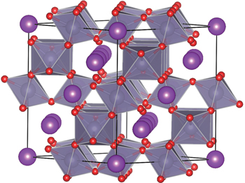
Fig. 1. Crystal structure of the pyrochlore-type γ-Bi2Sn2O7. The octahedrons sharing vertices represent SnO6 subunits, where Sn atoms are located in the center and O atoms at the vertices.
Table 1.

Optimized structural parameters of γ-Bi2Sn2O7. The experimental values[24] are given in the following parentheses for comparison.

.
3.2. Electronic and optical properties

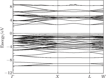
The calculated electronic band structure of γ-Bi2Sn2O7 is plotted in Fig. 2. The valence band maximum (VBM) is located at the X point and the conduction band minimum (CBM) is at the Γ point in the Brillouin zone and the Fermi level (EF) is at the top of the valence band, which means that the pyrochlore-type Bi2Sn2O7 is the p-type semiconductor with an indirect gap. The calculated band gap is about 2.72 eV and agrees well with the experimental data (2.78 eV)[12] and previously calculated value (2.74 eV).[15] The bands near EF are relatively flat and possess a high concentration of carriers, which is beneficial for light absorption. The calculated values of the effective mass of carrier (m*) are listed in Table 2 and helpful to understand the electrical properties of γ-Bi2Sn2O7. The effective mass values in different directions are identical, indicating isotropic electric behavior of cubic γ-Bi2Sn2O7. The effective mass of hole is obviously heavier than that of electron regardless of being at Γ or the X point, which shows that the electrons play a major role in determining the electrical conductivity for γ-Bi2Sn2O7.

Fig. 2. Calculated electronic band structure of γ-Bi2Sn2O7 along the selected high symmetry lines. The Fermi level is set to be zero for reference.

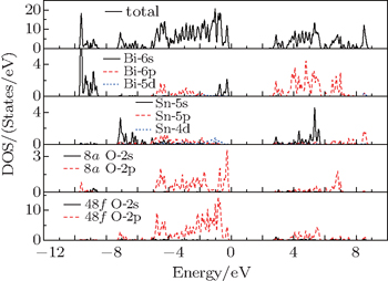
Figure 3 shows the total and partial density of states (DOS) of γ-Bi2Sn2O7. The valence bands (VBs) centered at about −9.2 eV are mainly from the 6s states of Bi atoms and the 2s and 2p states of O (8a) atoms. The VBs approximately ranging from −7.4 eV to −5.3 eV are formed mainly due to the hybridization between the 5s states of Sn atoms and the 2p states of O (48 f) atoms. In the energy region from about −5.2 eV to −1.6 eV, the total DOS is mainly from the Bi-6p, Sn-5p, O (8a)-2p, and O (48 f)-2p states. The hybridization interaction between Sn-4d and O (48f)-2p states is also obvious in a narrow energy region from −1.4 eV to −0.5 eV. The VBs in the energy region from −0.9 eV up to the EF are mainly comprised of the Bi-6s, O (8a)-2p, and O (48f)-2p states, and essential to determining the electrical properties of γ-Bi2Sn2O7. It can also be found from Fig. 3 that the conduction bands (CBs) close to the CBM are mainly created with the Bi-6p, Sn-5s, O (8a)-2p,and O (48 f)-2p states.

Table 2.

Calculated effective mass tensors of electrons in the conduction band and holes in the valence band near the EF at Γ (0, 0, 0) and X (0.5, 0, 0.5) points as marked in Fig. 1. All values are in units of free electron mass m0.

.
Fig. 3. Calculated total and partial DOS of γ-Bi2Sn2O7.

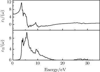
Figure 4 shows the calculated real part ε1(ω) and imaginary part ε2(ω) of the complex dielectric function for cubic γ-Bi2Sn2O7, each as a function of photon energy up to 35 eV. The static dielectric function is found to be 5.5 at 0 eV. The origin of the observed peak in the imaginary part ε2(ω) of the dielectric function can be explained with the help of the calculated DOS shown in Fig. 3, since ε2(ω) is correlated to the crystal absorption spectrum. The first two stronger absorption peaks centered at about 3.7 eV and 5.6 eV in ε2(ω) are probably ascribed to the transitions from the occupied states of the valence band group to the unoccupied electronic states at the bottom of the conduction band (CB).

Fig. 4. Calculated dependences of real part ε1(ω) and imaginary part ε2(ω) of the dielectric function of γ-Bi2Sn2O7 alloys on photon energy.

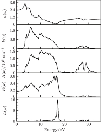
Based on the obtained dielectric function, the refractive index n(ω), extinction coefficient k(ω), absorption coefficients α(ω), reflectivity R(ω), and electron energy-loss function L(ω) are further calculated to check the optical properties of γ-Bi2Sn2O7 (see Fig. 5). The static refractive index n(0) is about 2.4, which is closely related to the real part ε1(ω) of the dielectric function. n(ω) reaches its maximum value of 3.6 at 3.5 eV and then drops drastically with the increase of photon energy. The calculated k(ω) is below 0.1 in a photon energy range from 0 to about 3 eV, meaning that γ-Bi2Sn2O7 will have a response to the light with wavelength less than 414 nm. Then k(ω) increases rapidly with increasing photon energy, forms the first peak in the near UV region at approximately 4.1 eV, and reaches the maximum value of about 2.1 at 5.8 eV. Our calculated results indicate that cubic γ-Bi2Sn2O7 has strong extinction effects on the part of violet light in the visible light region, the part near the UV region, and most of the part of the far UV region. The calculated absorption intensity of α(ω) in the infrared and most visible region is nearly zero and starts to go up rapidly at about 2.5 eV. There is a broad absorption peak ranging from about 3.7 eV to 25 eV. Especially, the first two strong peaks at about 6.2 eV and 9.8 eV are related to the transitions of Sn-5s and Bi-6s orbitals. The majority of the absorption spectrum of cubic Bi2Sn2O7 is in the UV region, which suggests that cubic Bi2Sn2O7 may have special applications in certain optical components. The calculated R(ω) shows that the average reflectivity is about 30%, which is an acceptable value for light absorbing material. Two small peaks at about 27.6 eV and 29.1 eV except the strong main peak at about 16.9 eV in the calculated L(ω) presented in Fig. 5 can be found, which corresponds to the energy of the plasma edge and shows the characteristics of plasma oscillation in γ-Bi2Sn2O7.

Fig. 5. Calculated refractive index n(ω), extinction coefficient k(ω), absorption coefficient α(ω), reflectivity R(ω), and electron energy-loss function L(ω) of γ-Bi2Sn2O7, each as a function of photon energy.
3.3. Mechanical properties

The calculated elastic constants Cij of γ-Bi2Sn2O7 are listed in Table 3.

Table 3.

Calculated values of elastic constant Cij, bulk modulus B, shear modulus G, Young’s modulus E, and Poisson’s ratio υ of γ-Bi2Sn2O7.

.

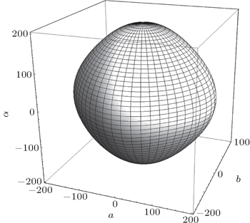
The bulk modulus B and shear modulus G are obtained by Voigt–Reuss–Hill approximation.[25] Young’s modulus E and Poisson’s ratio υ can be further calculated according to their relationships with B and G. The corresponding mechanical stability criterion for cubic crystal is that B, C11C12, and C44 are positive.[26] It can be found from Table 3 that γ-Bi2Sn2O7 satisfies the condition for elastic stability. The calculated B and G of γ-Bi2Sn2O7 are 158.2 GPa and 73.8 GPa respectively, and the value of B/G is about 2.14, obviously indicating that cubic Bi2Sn2O7 belongs to a kind of ductile material, since the material is ductile if its B/G value is higher than 1.75 according to Pugh’s criteria of brittleness and ductility.[27] Furthermore, the calculated Poisson’s ratio is about 0.3 and also shows the ductile characteristic of cubic Bi2Sn2O7. According to Zener’s definition,[28] the anisotropy of material can be described by the parameter A = G1/G2, where G1 = C44, G2 = (C11C12)/2. Generally, the isotropic material has a value of A = 1. For γ-Bi2Sn2O7, the calculated A is about 0.96, showing high isotropy. In addition, according to the relationship between Young’s modulus and elastic compliance constants,[29] the elastic anisotropy of γ-Bi2Sn2O7 can be directly checked by the directional dependence of Young’s modulus. The calculated results depicted in Fig. 6 show that the directional dependence of Young’s modulus almost exhibits a spherical shape, which indicates that γ-Bi2Sn2O7 is highly isotropic.

Fig. 6. Directional dependence of Young’s modulus of cubic γ-Bi2Sn2O7.
4. Conclusions

The electronic, optical, and mechanical properties of γ-Bi2Sn2O7 are investigated by using the first-principles DFT calculations. Our results show that γ-Bi2Sn2O7 is the p-type semiconductor with an indirect band gap. The calculated band gap is about 2.72 eV and in excellent agreement with the experimental result. The hybridization interaction between Bi-6s and O-2p states in the valence bands close to the Fermi level is expected to play an essential role in determining the electrical behavior of γ-Bi2Sn2O7. The dielectric function and macroscopic optical constants including refractive index, extinction coefficient, absorption coefficients, reflectivity, and electron energy-loss function are also calculated to check the optical properties of γ-Bi2Sn2O7. Especially, the average reflectivity is about 30%, which indicates that γ-Bi2Sn2O7 is a good light absorbing material used for optical semiconductor devices and photocatalysts. Moreover, γ-Bi2Sn2O7 is mechanically stable and ductile according to the calculated elastic constants, bulk modulus, Young’s modulus, and Poisson’s ratio. The further calculations of the directional dependence of Young’s modulus show that γ-Bi2Sn2O7 is highly isotropic.

Reference
1Abe RHigashi MZou ZSayama KAbe Y 2004 Chem. Lett. 33 954
2Park SSong HChoi HMoon J 2004 Solid State Ionics 175 625
3Bramwell S TGingras M J P 2001 Science 294 1495
4Hanawa MMuraoka YTayama TSakakibara TYamamura JHiroi Z 2001 Phys. Rev. Lett. 87 187001
5Roth R S 1956 J. Res. Nat. Bur. Stand. 56 17
6Brisse FKnop O 1968 Can. J. Chem. 46 859
7Subramaniam M AAravamudan GSubba Rao G V 1983 Prog. Solid State Chem. 15 55
8Kahlenberg VZeiske T1997Z. Kristallogr.212297
9Gao FChen X YYin K BDong SRen Z FYuan FYu TZou Z GLiu J M 2007 Adv. Mater. 19 2889
10Tang J WZou Z GYe J H 2004 Catal. Lett. 92 53
11Yu JKudo A 2006 Adv. Funct. Mater. 16 2163
12Wu JHuang F XChen PWan DXu F 2011 J. Mater. Chem. 21 3872
13Tian QZhuang JWang JXie LLiu P2012Appl. Catal. A: Gen.425–42674
14Xu WFang JZhu XFang ZChen C 2015 Mater. Res. Bull. 72 229
15Walsh AWatson G W 2007 Chem. Mater. 19 5158
16Fan WHu JHuang JWu XLin SHuang CQiu X 2015 Appl. Surf. Sci. 357 2364
17Kresse GJoubert D1999Phys. Rev. B591758
18Kresse GHafner J 1994 Phys. Rev. 49 14251
19Kresse GFurthmüller J 1996 Comput. Mater. Sci. 6 15
20Perdew J PBurke KErnzerhof M 1996 Phys. Rev. Lett. 77 3865
21Monkhorst H JPack J D 1976 Phys. Rev. 13 5188
22Adolph BFurthmüller JBechstedt F 2001 Phys. Rev. 63 125108
23Gajdoš MHummer KKresse GFurthmüller JBechstedt F 2006 Phys. Rev. 73 045112
24Kahlenberg VZeiske T Z1997Z. Kristallogr.212297
25Hill R 1952 Proc. Phys. Soc. London 65 349
26Wallace D C1972Thermodynamics of CrystalsNew YorkWiley
27Pugh S F 1954 Philos. Mag. 45 823
28Zener C1948Elasticity and Anelasticity of MetalsChicagoUniversity of Chicago Press
29Ranganathan S IOstoja-Starzewski M 2008 Phys. Rev. Lett. 101 055504