Modulation of physical properties of oxide thin films by multiple fields
Yang Hua-Li1, 2, Wang Bao-Min1, 2, †,  , Zhu Xiao-Jian1, 2, Shang Jie1, 2, Chen Bin1, 2, Li Run-Wei1, 2, ‡,
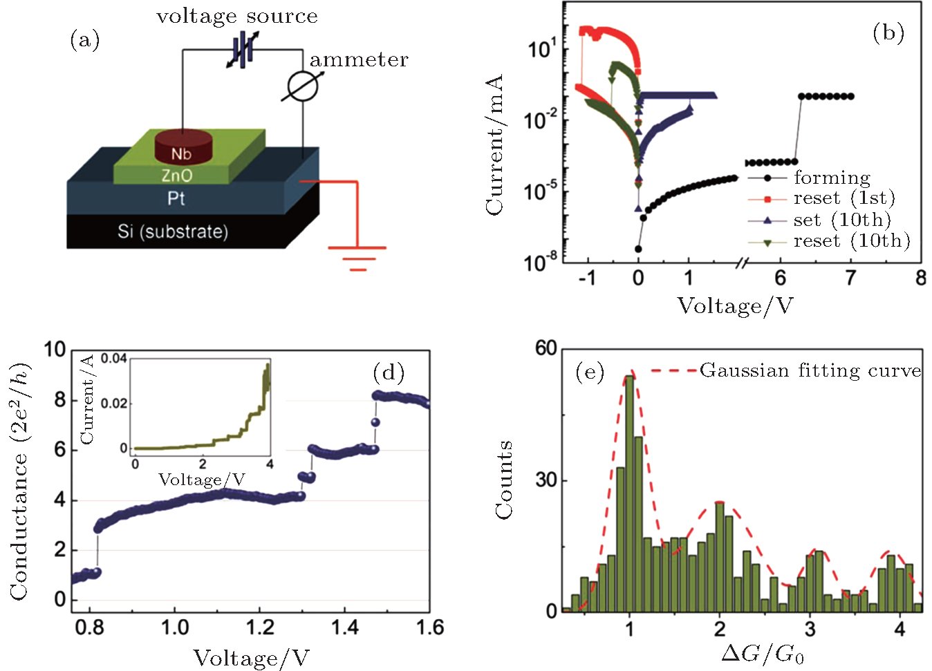
, Zhu Xiao-Jian1, 2, Shang Jie1, 2, Chen Bin1, 2, Li Run-Wei1, 2, ‡, (a) Schematic of a sandwiched Nb/ZnO/Pt structure. (b) Typical bipolar RS behaviors observed in the device. (c) Measured conductance as a function of the bias voltage during the set process. Inset: Corresponding