Yang Hua-Li 1, 2, Wang Bao-Min 1, 2, †,  , Zhu Xiao-Jian 1, 2, Shang Jie 1, 2, Chen Bin 1, 2, Li Run-Wei 1, 2, ‡, |
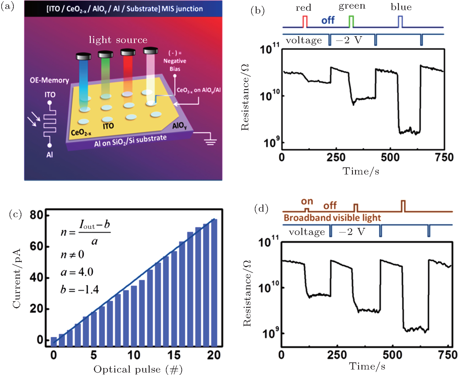
(a) Schematic diagram of the ITO/CeO2−x/AlOy/Al junction structure and the operating principle of a multifunctional optoelectronic RS memory (OE-Memory). (b) Wavelength-dependent photoresponse of the device upon being exposed to monochromic illumination with the wavelength of 638 nm, 560 nm or 499 nm at the same intensity of 6 pW/μm2, respectively, enables the device as a optoelectronic demodulator. (c) Stepwise and linear relationship between the device output current and the number of the input light pulses, which forms the basis for applications of computing functions. The read voltage is 0.1 V. Iout, n, a, and b stand for the output current (pA) of the device, number of light pulse inputs, photocurrent ramping step of ∼4.0 (pA) per light illumination, and a constant of ∼ −1.4 (pA), respectively, for n ≠ 0. The dark current is ∼2 pA for n = 0. (d) Intensity-dependent photoresponse of the device under broadband illumination with the intensities of 8 pW/μm2, 21 pW/μm2, and 60 pW/μm2, respectively, renders promising multilevel storage capabilities.[259] |