Properties of n-Ge epilayer on Si substrate with
Huang Shi-Hao1, †,  , Li Cheng2, Chen Cheng-Zhao3, Wang Chen2, Xie Wen-Ming1, Lin Shu-Yi1, Shao Ming1, Nie Ming-Xing1, Chen Cai-Yun1
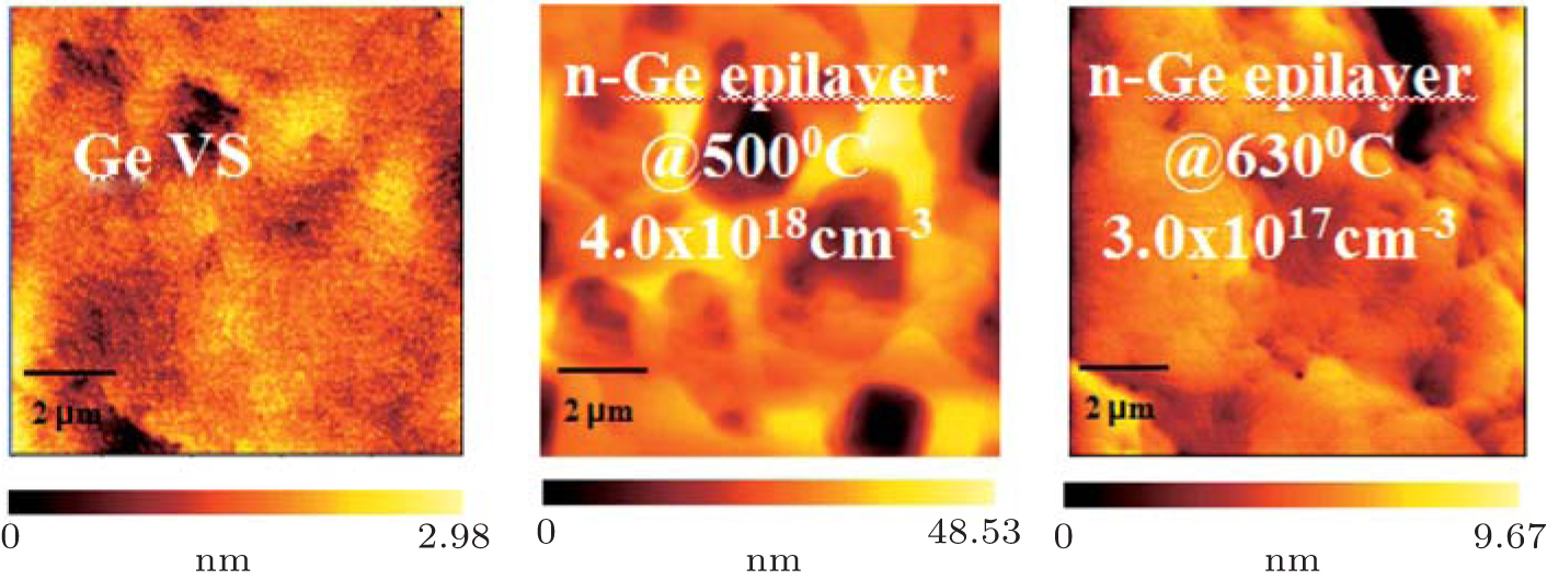
, Li Cheng2, Chen Cheng-Zhao3, Wang Chen2, Xie Wen-Ming1, Lin Shu-Yi1, Shao Ming1, Nie Ming-Xing1, Chen Cai-Yun1 Typical surface morphology images of the Ge VS grown on Si, n-Ge epilayers at growth temperatures of 500 °C and 630 °C with doping concentrations of 4.0 × 1018 cm−3 and 3.0 × 1017 cm−3 respectively. The root mean square surface roughness values of the three samples are 0.45 nm, 6.50 nm, and 1.50 nm within 10 μm × 10 μm AFM images respectively.