Distribution of electron traps in SiO2/HfO2 nMOSFET
Hou Xiao-Hui1, Zheng Xue-Feng2, †,  , Wang Ao-Chen2, Wang Ying-Zhe2, Wen Hao-Yu2, Liu Zhi-Jing1, Li Xiao-Wei2, Wu Yin-He2
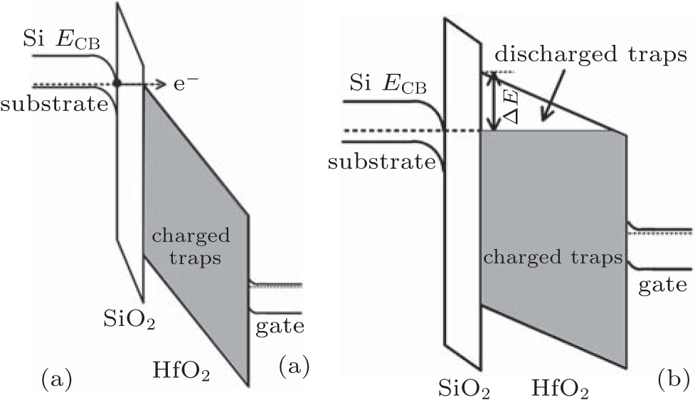
, Wang Ao-Chen2, Wang Ying-Zhe2, Wen Hao-Yu2, Liu Zhi-Jing1, Li Xiao-Wei2, Wu Yin-He2 The schematic energy band diagrams of nMOSFET with SiO2/HfO2 gate dielectric for (a) charging at high positive gate bias and (b) discharging at lower gate bias, respectively.