

First-principles investigation of electronic structure, effective carrier masses, and optical properties of ferromagnetic semiconductor CdCr2S4
[Zhu Xu-Hui1, 2, Chen Xiang-Rong1, 3, †,  , Liu Bang-Gui2, ‡, ]
, Liu Bang-Gui2, ‡, ]
|
|


† Corresponding author. E-mail:
‡ Corresponding author. E-mail:
Project supported by the Joint Fund of the National Natural Science Foundation of China and the China Academy of Engineering Physics (Grant Nos. U1430117 and U1230201).
The electronic structures, the effective masses, and optical properties of spinel CdCr2S4 are studied by using the full-potential linearized augmented planewave method and a modified Becke–Johnson exchange functional within the density-functional theory. Most importantly, the effects of the spin–orbit coupling (SOC) on the electronic structures and carrier effective masses are investigated. The calculated band structure shows a direct band gap. The electronic effective mass and the hole effective mass are analytically determined by reproducing the calculated band structures near the BZ center. SOC substantially changes the valence band top and the hole effective masses. In addition, we calculated the corresponding optical properties of the spinel structure CdCr2S4. These should be useful to deeply understand spinel CdCr2S4 as a ferromagnetic semiconductor for possible semiconductor spintronic applications.
Recently, the ferromagnetic semiconductive spinel compounds have been studied for potential candidates for semiconductor spintronic devices.[1–5] A great deal of experimental attention has been concentrated on the cubic spinel compound CdCr2S4. In 2005, Hemberger et al.[1] reported that the cubic spinel CdCr2S4 has relaxor-like dielectric properties and colossal magnetocapacitance. Sun et al.[6] observed several interesting behaviors in spinel system CdCr2S4, showing that a glassy dipolar state occurs near TC ∼ 85 K and a ferroelectric ordering occurs near Tp ∼ 56 K. Gnezdilov et al.[7] showed pronounced phonon anomalies indicating a symmetry reduction and Cr off-centering in the cubic unit cell of CdCr2S4. Subsequently, Oliveira et al.[8] demonstrated that a linear coupling between the magnetic and polar order parameters is sufficient to justify the appearance of a magnetic cluster in the paramagnetic phase of CdCr2S4. Furthermore, using muon spin rotation/relaxation spectroscopy (μSR), Hartmann et al.[9] studied the magnetic properties of CdCr2S4.
On the theoretical side, with an ab initio method, Shanthi et al.[10] calculated the electronic structures for both the nonmagnetic and the ferromagnetic states of CdCr2S4, and presented that CdCr2S4 corresponds to a ferromagnetic semimetallic ground state, with very low density of states at the Fermi energy and a nearly gapped structure. Fennie et al.[11] studied the dielectric properties, zone-center phonons and Born effective charges of the ferromagnetic spinel CdCr2S4. In the same year, Lunkenheimer et al.[12] provided strong evidence that the variation of the dielectric constant at the magnetic transition and the colossal MC effect in this material are caused by a speeding up of relaxation dynamics under the formation of the magnetic order. In 2008, within the local spin-density approximation LSDA and LSDA+U, Yaresko[13] obtained the semiconductive electronic band structure and exchange coupling constants in CdCr2S4 spinels. Recently, using a modified Becke–Johnson (mBJ) exchange plus local density approximation correlation, Guo et al.[14] obtained accurate energy gaps and optical properties of ferromagnetic semiconductors CdCr2S4. However, more theoretical investigation is needed for achieving more insights of the ferromagnetic semiconductor spinel material.
Here, we use the full-potential density-functional-theory method to investigate the electronic structures, effective carrier masses, and optical functions of the CdCr2S4, with the spin–orbit coupling taken into account and the semiconductor gap accurately calculated. This paper is organized as follows. The theoretical methods and computational details are given in Section 2. Our calculated results and some discussions are presented in Section 3. Finally, a summary of our main results is given in Section 4.
The electronic structures of ferromagnetic semiconductor CdCr2S4 in spinel structure were carried out by using a full potential linearized augmented plane waves (FPLAPW) method in the framework of the DFT[15,16] as implemented in the Wien2k package.[17,18] We use a modified Becke–Johnson (mBJ) semi-local exchange potential[19] plus the local density approximation (LDA) for the correlation potential[20,21] to do our main DFT calculations, and additionally do some calculations with the popular generalized gradient approximation (GGA)[22] for necessary comparison. It is well known that the mBJ exchange plus LDA correlation can produce accurate semiconductor gaps for semiconductors and insulators[14,20,23–26] and overcome the usual LDA and GGA underestimation of the band gaps. The full relativistic effects are calculated with the Dirac equations for core states, and the scalar relativistic approximation is used for valence states.[27–29] The spin–orbit coupling (SOC) is taken into account. The maximum l quantum number for the wave function expansion inside atomic spheres was set to lmax = 10. The convergence parameter Rmt × Kmax is set to 8 and the radii Rmt of the atomic spheres are chosen as 2.47 (Cd), 2.43 (Cr), and 2.05 (S) Bohr for CdCr2S4. We use 1000 k-points in the first Brillouin zone for self-consistent calculation and 10000 k-points for optical properties calculation. The self-consistent calculations are considered to be converged only when the integration of the absolute charge-density difference between the input and output electron density is less than 0.0001|e| per formula unit, where e is the electron charge.
CdCr2S4 is a typical ferromagnetic semiconductor with the spinel structure AB2X4, which belongs to the space group 227 (Fd-3m). The primitive cell crystal structure is shown schematically in Fig.
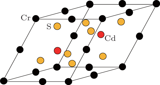 | Fig. 1. The primitive cell structure of spinel CdCr2S4. |
| Table 1. The lattice constants (a), primitive cell volume (V), semiconductor energy gap (Eg) and the magnetic moment (M) in the spinel ferromagnetic semiconductor CdCr2S4. . |
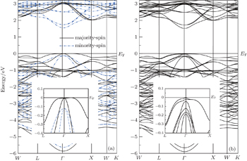
To overcome LDA and GGA underestimation of energy gaps, we have used the mBJ approximation. The electronic band structures for the spinel structure CdCr2S4 along the high symmetry directions in the first Brillouin zone are calculated. The effect of the spin–orbit coupling is investigated. In Fig.
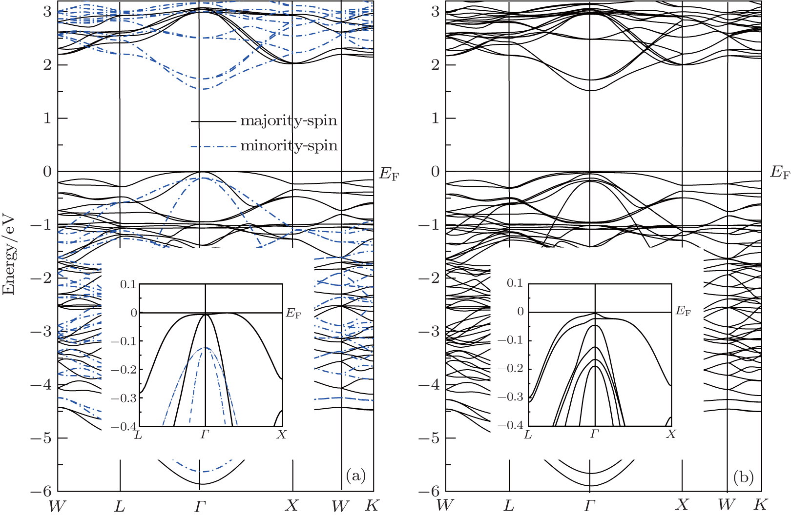 | Fig. 2. Energy bands of CdCr2S4 calculated with mBJ (a) and with mBJ-SOC (b). |
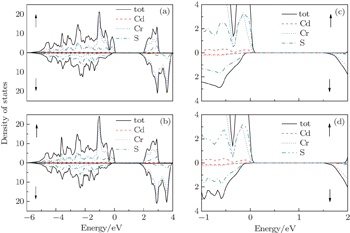
Furthermore, we have calculated the total density of states (TDOS) of CdCr2S4 between −6 eV and 4 eV with both mBJ and mBJ plus SOC, and present the results in Figs.
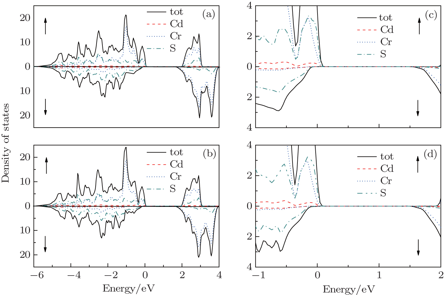 | Fig. 3. The spin-resolved total density of states ((a) mBJ, (b) mBJ-SOC) and the amplified parts near the Fermi energy ((c) mBJ, (d) mBJ-SOC) of CdCr2S4. |
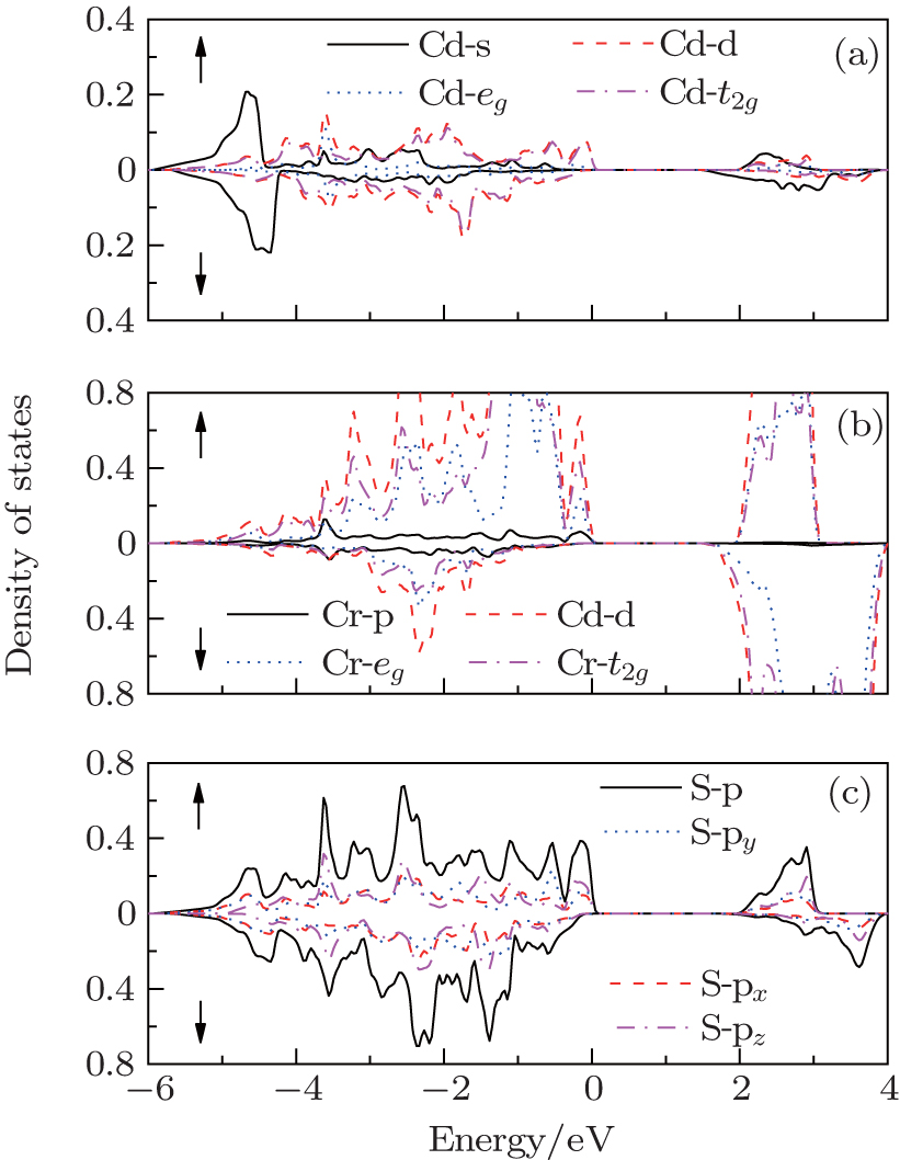 | Fig. 4. The spin-resolved partial density of states of CdCr2S4 with mBJ-SOC: (a) Cd s and Cd d electrons; (b) Cr p and Cr d electrons; (c) S p electrons. |
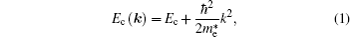
The electronic structures of a semiconductor near the band valence top and the conduction band bottom are vital to its electronic transport properties. The effective mass theory will undoubtedly become one of the direct ways to understand the material properties. If the band extremum is located in the center of the Brillouin zone, the band dispersion function E(p) should be parabolic for a small p value. Using effective mass approximation theory, the dispersion relation near the conduction band minimum (CBM) can be written as
Without the spin–orbit coupling, we use 1000 points along three main high-symmetry directions: [001], [110], and [111] in the first Brillouin zone, then fit the 0.5% range of the dispersion curves near the CBM and VBM by using Eq. ( along the three directions near the Γ point. The results are presented in Tables
along the three directions are almost the same, which means that the electron effective mass is isotropic in the k space. It can be seen in Table
and
. Unlike the electron effective mass, the hole effective mass is anisotropic in the k space.
| Table 2. The electron effective masses along [001], [110], and [111] directions of CdCr2S4 calculated by mBJ and mBJ-SOC. . |
| Table 3. The hole effective masses |
The spin–orbit coupling changes substantially the band structures. There appears a spin–orbit splitting band near VBM. We also choose 1000 points along the three high-symmetry directions, [001], [110], and [111], in the first Brillouin zone, and fit the 0.5% range of the dispersion relation near the CBM and VBM. The final fitting results are presented in Tables in Table
,
, and
. As the band structures show, the heavy hole in the majority-spin channel is very anisotropic near the center of the Brillouin zone, and in contrast, the other holes are substantially less anisotropic. In addition, the spin–orbit coupling makes the heavy holes much more heavy and the light holes lighter, and on the other hand it enhances the anisotropy of the heavy holes.
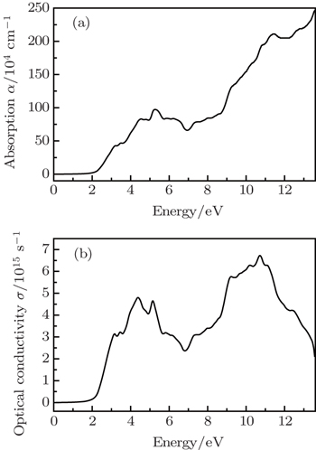
Ambrosch-Draxl et al.[35] have pointed out that the random phase approximation (RPA) is a useful method to calculate the screening and optical response in solids. They have provided formalism for treating optical properties within the RPA and implemented it with the Wien2k package.[17,18] Werner et al.[36] have successfully calculated the optical constants for 17 elemental metals with this method. The complex dielectric function of a solid is given as ε(ω) = ε1(ω) + iε2(ω) to describe the optical response of the material at photon energy ω. The imaginary part, ε2(ω), includes contributions from both of the spin channels. The real part, ε1(ω), can be extracted from the imaginary part using the Kramers–Kronig relation. The other optical coefficients can be expressed in terms of the dielectric function. Using the definition of direct transition and Kramers–Kronig relation,[37] we calculated optical properties of CdCr2S4 in the spinel cubic phase with mBJ calculation. Our calculated real and imaginary parts of the dielectric functions ε for CdCr2S4 are consistent with the result in the previous work.[14] The other optical properties are also studied. We present the optical absorption coefficient α(ω) and optical conductivity σ(ω) as functions of the photon energy in Fig.
 | Fig. 5. The optical absorption coefficient α(ω) (a) and conductivity σ(ω) (b) as a function of photon energy for CdCr2S4. |
In summary, the electronic structures and effective mass of ferromagnetic semiconductor CdCr2S4 have been investigated by using the full-potential linearized augmented plane wave (FP-LAPW) method within the density-functional theory. We use the modified Becke–Johnson (mBJ) exchange functional to accurately describe the electronic structures, especially the semiconductor gap, of ferromagnetic semiconductor CdCr2S4 and investigate the effects of the spin–orbit coupling. The calculated band structure shows a direct band gap, which accords well with the previous theoretical results and the experimental findings. The contribution of different bands was analyzed from the total and the partial density of states curves. The electronic effective mass and the hole effective masses are analytically determined by reproducing the calculated band structures near the Brillouin zone center on the basis of the effective-mass Hamiltonian. In addition, the important optical properties are investigated. These should be useful to study carrier transport properties of ferromagnetic semiconductor CdCr2S4 and similar magnetic semiconductors.
| 1 | |
| 2 | |
| 3 | |
| 4 | |
| 5 | |
| 6 | |
| 7 | |
| 8 | |
| 9 | |
| 10 | |
| 11 | |
| 12 | |
| 13 | |
| 14 | |
| 15 | |
| 16 | |
| 17 | |
| 18 | |
| 19 | |
| 20 | |
| 21 | |
| 22 | |
| 23 | |
| 24 | |
| 25 | |
| 26 | |
| 27 | |
| 28 | |
| 29 | |
| 30 | |
| 31 | |
| 32 | |
| 33 | |
| 34 | |
| 35 | |
| 36 | |
| 37 |