Effect of supply voltage and body-biasing on single-event transient pulse quenching in bulk fin field-effect-transistor process
Yu Jun-Ting1, Chen Shu-Ming1, 2, †,  , Chen Jian-Jun1, Huang Peng-Cheng1, Song Rui-Qiang1
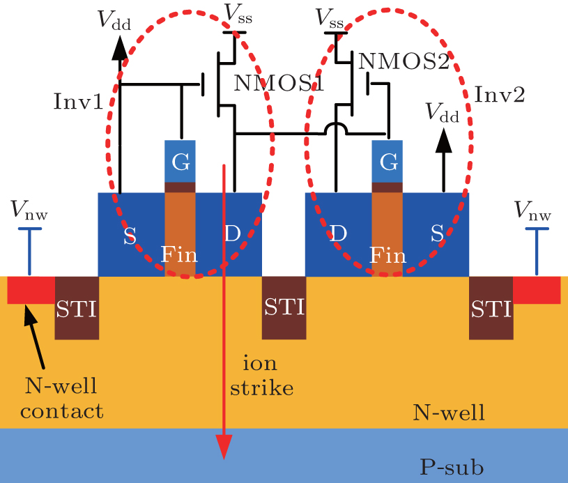
, Chen Jian-Jun1, Huang Peng-Cheng1, Song Rui-Qiang1 Schematic configuration of the mixed-mode simulation setup for a two-stage inverter chain. The TCAD p-FinFETs are cut in the middle of the gate along the source/drain direction (