Numerical simulation of the magnetoresistance effect controlled by electric field in p–n junction
Yang Pan, Chen Wen-Jie, Wang Jiao, Yan Zhao-Wen, Qiao Jian-Li, Xiao Tong, Wang Xin, Pang Zheng-Peng, Yang Jian-Hong†,
       

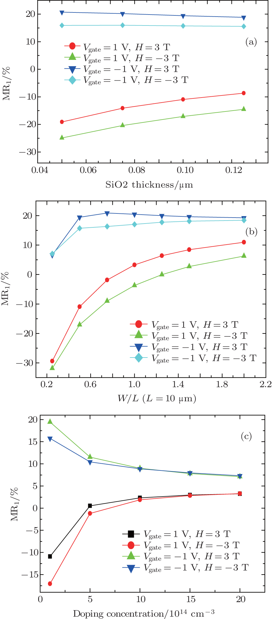
Variations of MR1 with (a) SiO2 thickness with W = 5 μm, L = 10 μm, and NA = ND = 1×1014 cm−3, (b) W/L with SiO2 thickness d = 0.1 μm, L = 10 μm, and NA = ND = 1×1014 cm−3, (c) doping concentration (NA = ND) with W = 5 μm, L = 10 μm, and NA = ND = 1×1014 cm−3. A bias voltage of 0.9 V is applied at T = 300 K under conditions in panels (a), (b), and (c).